An open-access map of the entire silicon value chain
Silicon University documents semiconductor manufacturing end to end, from quartzite reduction chemistry to copper hybrid bonding, as a tiered curriculum anyone can follow.
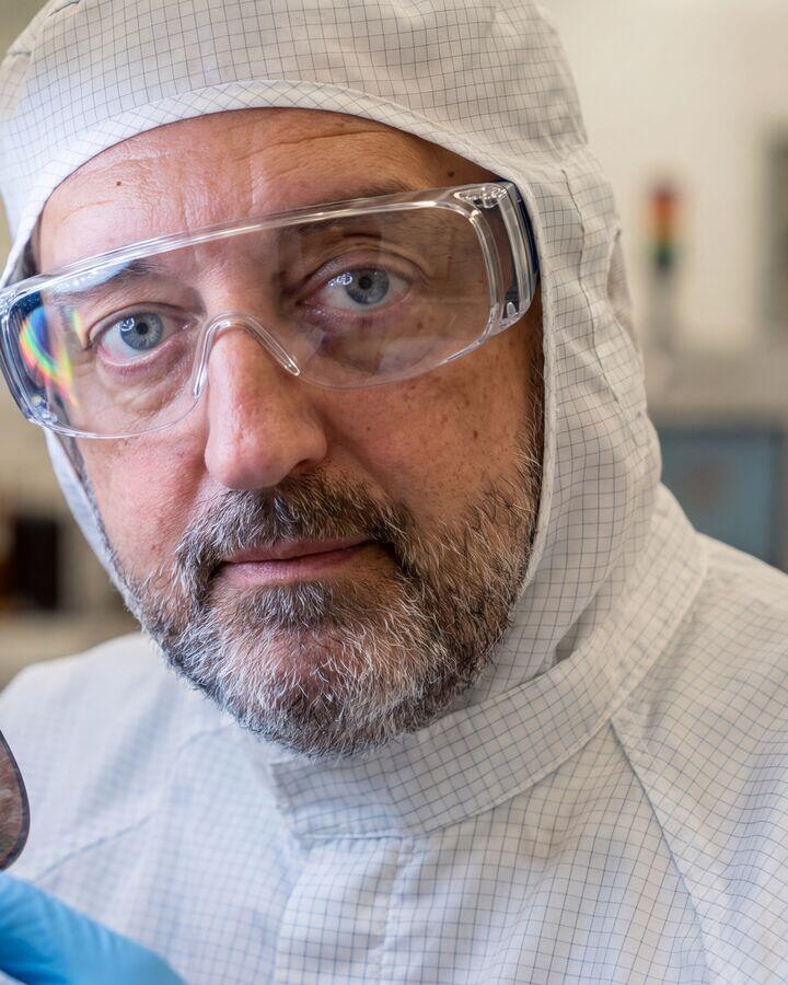
Dimitri Albino
Project Leader, Advanced Wet Processing Equipment Manufacturing & Deployment. Dimitri curates every article of the curriculum and grounds it in day-to-day fab practice: tool kinematics, bath chemistry, defectivity data and yield transfer.
Two tracks, eight pillars, three tiers
The same body of knowledge, three ways in: a chronological fab journey, a practitioner matrix, and a tier system that tells you how deep a page goes.
The Guided Fab Journey
24 steps follow one silicon atom from quartzite to packaged device. Start step 01 →
The Practitioner Matrix
Every article indexed by pillar, topic and tier for direct jump-in. Browse the matrix →
Depth Control
Fundamentals, equipment kinematics, then quantitative yield engineering, for every topic. How tiers work →
Written like process documentation, not marketing
Numbered sections, real equations, parameter tables, schematics and source diagrams. Each article carries a defined scope, audience and prerequisite chain.