From quartzite sand to sub-2nm processors
A practitioner-guided curriculum for semiconductor manufacturing: two learning tracks, eight fab pillars, three depth tiers, 72 articles from bulk crystal to heterogeneous integration.
Curated by Dimitri Albino, Project Leader, Advanced Wet Processing Equipment Manufacturing & Deployment.
Built by a fab practitioner, for future fab practitioners
Silicon University is an independent, open-access editorial project covering the silicon value chain end to end. The curriculum follows a single silicon atom from quartzite mining chemistry to a packaged 2.5D/3D device, with equipment kinematics, quantitative process windows and yield engineering at every step.
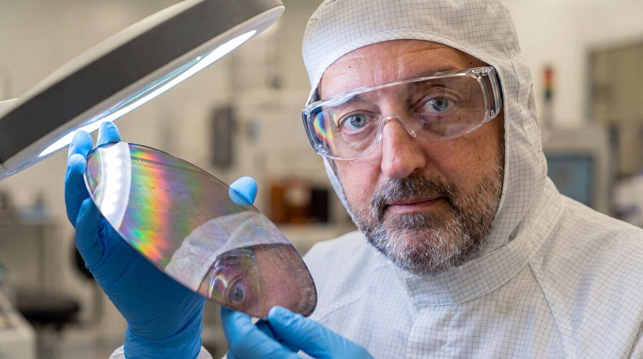
Learn it in order, or jump straight to your problem
Track A follows a single silicon atom through the fab in 24 guided steps. Track B is a faceted matrix built for practitioners who already know where they are heading.
A guided, linear, zero-to-hero path. Twenty-four steps, each at three depth tiers, from carbothermic reduction to hybrid bonding.
Quartzite Extraction & Carbothermic Reduction
Quartzite02Chemical Purification & the Siemens Process
Quartzite03Monocrystalline Growth: Czochralski & Float Zone
Quartzite04Ingot Mechanical Processing & Geometric Conditioning
Ingot05Multi-Wire Diamond Sawing & Wafer Slicing
Ingot06Edge Profiling, Lapping & Stress-Relief Etching
Ingot07Oxide & Polysilicon CMP
Wafering08Copper Damascene & Barrier CMP
Wafering09Slurry, Pad Conditioning & CMP Metrology
Wafering10RCA Wet Cleans & Dilute Chemistry
FEOL11Wet Bench vs Single-Wafer Processing
FEOL12Particle Removal & Zeta Potential Engineering
FEOL13DUV Immersion Lithography (193i)
FEOL14EUV & High-NA EUV Lithography
FEOL15Computational Lithography & OPC
FEOL16Reactive Ion Etching & Plasma Physics
FEOL17Atomic Layer Etching
FEOL18High-Aspect-Ratio Plasma Etching
FEOL19Thermal Oxidation & Gate Dielectric Growth
FEOL20ALD & High-k Metal Gate Stacks
FEOL21Ion Implantation & Thermal Annealing
FEOL22BEOL Metallization, Dual Damascene & Low-k
BEOL23TSVs, Wafer Thinning & Backside Power
Packaging24Hybrid Bonding & Chiplet Integration
PackagingThe Practitioner Matrix
A modular, expert jump-in. Every article is indexed by pillar, topic and tier, so you can enter at exactly the unit operation or failure mode you are debugging. No prerequisites enforced.
Three tiers, one taxonomy
Every article is tagged by tier, so you always know how deep the page goes before you commit your afternoon.
Core Fundamentals
The physics and vocabulary you need before touching a tool.
Equipment & Kinematics
How the hardware actually moves, heats, and dispenses.
Deep-Dive & Yield Engineering
Quantitative process windows, defectivity, and yield transfer.
Start at Tier 1 for any topic, then descend through the same pillar without losing the thread.
Eight pillars of the fab
The full body of knowledge, from substrate synthesis to heterogeneous integration. Each pillar carries three topics across three tiers.
Substrate Material Synthesis & Bulk Crystal Engineering
Quartzite Extraction & Carbothermic Reduction · Chemical Purification & the Siemens Process · Monocrystalline Growth: Czochralski & Float Zone
9 articles · Explore →PILLAR 02Ingot Conditioning, Wafering & Mechanical Damage Remediation
Ingot Mechanical Processing & Geometric Conditioning · Multi-Wire Diamond Sawing & Wafer Slicing · Edge Profiling, Lapping & Stress-Relief Etching
9 articles · Explore →PILLAR 03Planarization Tribology & Chemical Mechanical Polishing
Oxide & Polysilicon CMP · Copper Damascene & Barrier CMP · Slurry, Pad Conditioning & CMP Metrology
9 articles · Explore →PILLAR 04Surface Chemistry, Ultra-Clean Wet Processing & Contamination Control
RCA Wet Cleans & Dilute Chemistry · Wet Bench vs Single-Wafer Processing · Particle Removal & Zeta Potential Engineering
9 articles · Explore →PILLAR 05Advanced Photolithography & Computational Optics
DUV Immersion Lithography (193i) · EUV & High-NA EUV Lithography · Computational Lithography & OPC
9 articles · Explore →PILLAR 06Plasma Etching & Atomic-Scale Material Removal
Reactive Ion Etching & Plasma Physics · Atomic Layer Etching · High-Aspect-Ratio Plasma Etching
9 articles · Explore →PILLAR 07Dielectric Deposition, Gate Stack Engineering & Thermal Processing
Thermal Oxidation & Gate Dielectric Growth · ALD & High-k Metal Gate Stacks · Ion Implantation & Thermal Annealing
9 articles · Explore →PILLAR 08BEOL Metallization, Advanced 2.5D/3D Packaging & Heterogeneous Integration
BEOL Metallization, Dual Damascene & Low-k · TSVs, Wafer Thinning & Backside Power · Hybrid Bonding & Chiplet Integration
9 articles · Explore →Where this curriculum lives
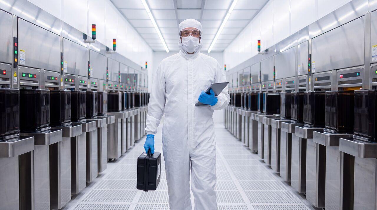
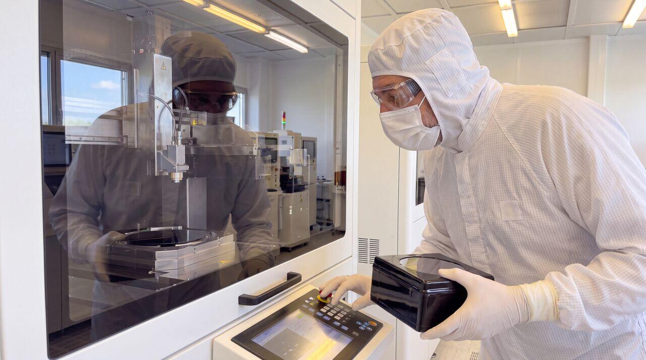
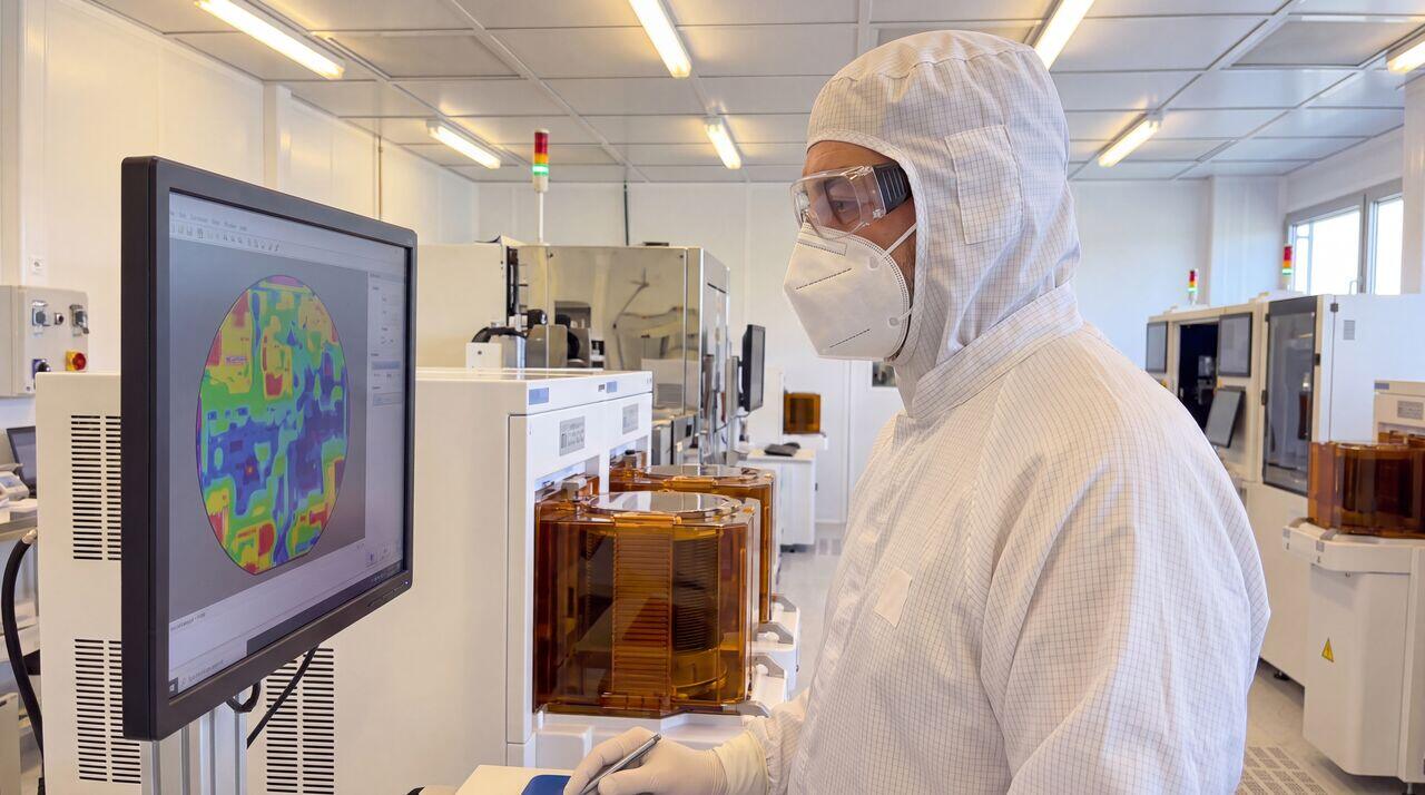
Production-cleanroom photography from the curator's own fab work. Every article keeps one foot on this floor.
DLVO Theory, Acoustic Cavitation Dynamics & Supercritical CO2 Drying Physics
Quantitative analysis of van der Waals (V_VDW) vs. Electrostatic Double Layer (V_EDL) interaction energy, Zeta potential (ζ) tuning across pH scales, stable acoustic micro-streaming vs. transient cavi…