01Beamline Architecture: From Ion Source to Wafer Target
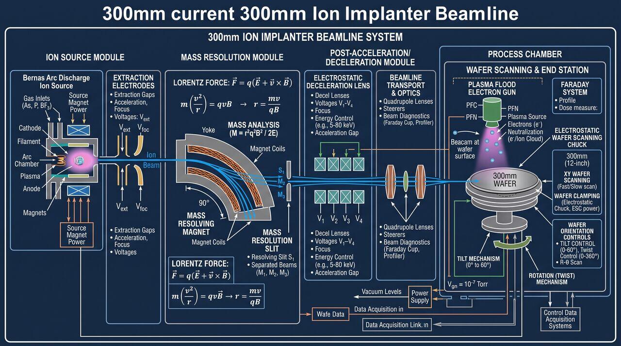
An advanced beamline ion implanter consists of five core subsystems operating under high vacuum ():
- Ion Source (Bernas or Indirectly Heated Cathode - IHC):
- Feeds precursor gases (, , ).
- A thermionic filament discharges electrons into the arc chamber, ionizing gas molecules into a dense plasma containing , , , and contaminant ions.
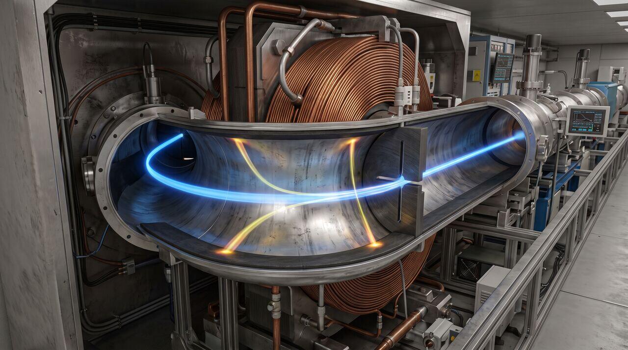
- Mass Analyzer Magnet:
- Uses a bending magnet to separate desired dopant species based on charge-to-mass ratio (m/q) according to the Lorentz force equation:
- Only ions with the exact specified mass-to-charge ratio pass through the resolving aperture; all unwanted contaminants collide with water-cooled graphite slits.
- Acceleration / Deceleration Lenses:
- Electrostatic lens arrays accelerate ions to final kinetic energies (up to for deep wells) or decelerate them down to sub-keV levels () for Ultra-Shallow Junctions (USJ).
- Plasma Flood Gun (Charge Neutralization):
- Implanting positive ions onto insulating dielectric layers ( or photoresist) creates massive surface charge buildup, leading to gate oxide electrostatic breakdown (ESD).
- The Plasma Flood Gun floods the wafer surface with low-energy secondary electrons, neutralizing positive surface charge completely.
- Process Endstation:
- Holds the wafer on an electrostatic tilt/twist chuck, enabling mechanical scanning or electrostatic beam scanning across the wafer surface with dose uniformity.
02Rapid Thermal Processing (RTP) & Spike Annealing Hardware
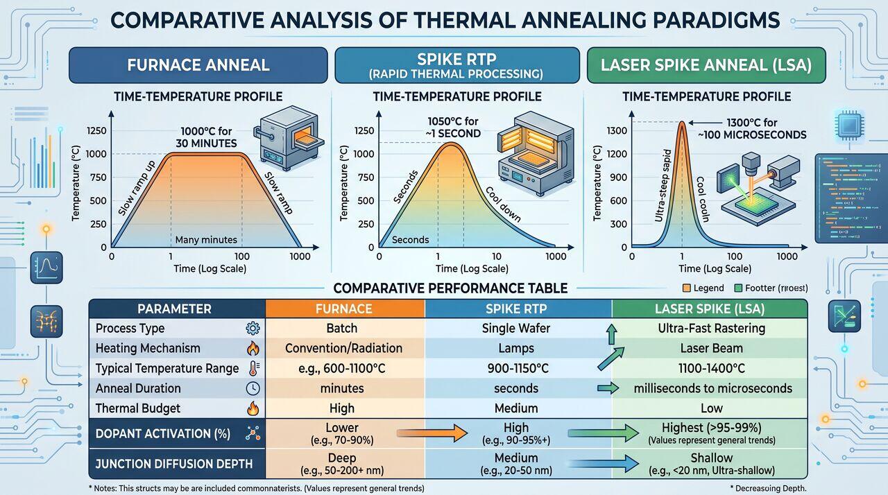
To activate dopants without allowing them to diffuse broadly (which would destroy ultra-short channel lengths), conventional long-duration furnace anneals () have been replaced by ultra-fast thermal tools:
Spike Anneal Temperature-Time ProfileSchematic · source diagram
- RTP Lamp Systems:
- Uses high-power tungsten-halogen or arc lamp arrays above and below the wafer, ramping temperature at rates exceeding to a peak spike temperature of with dwell times measured in milliseconds.
- Laser Spike Annealing (LSA) & Flash Lamp Annealing (FLA):
- To achieve sub-nanometer dopant activation for sub-2nm nodes, LSA scans a intense carbon dioxide or diode laser line across the wafer surface, heating only the top surface layer to for sub-millisecond durations (), achieving activation with zero bulk diffusion!
→Prerequisites & continue reading
Prerequisites: ["p07-t7.3-t1-ion-implantation-annealing-fundamentals"]
Also in Topic 7.3, Ion Implantation & Thermal Annealing:
Tier 1 · Ion Implantation & Thermal Annealing Fundamentals…Tier 3 · Ion Channeling, Transient Enhanced Diffusion (TED) &…