01Primary Dopants: Donors vs. Acceptors
Silicon belongs to Group IV of the periodic table with 4 valence electrons. Doping substitutes silicon atoms in the lattice with Group III or Group V elements:
- n-Type Doping (Donors - Extra Electrons):
- Phosphorus () & Arsenic (): Group V elements possessing 5 valence electrons. Inserting an arsenic atom supplies one free electron to the conduction band.
- Applications: NMOS source/drain regions, n-well contacts.
- p-Type Doping (Acceptors - Extra Holes):
- Boron ( or ): Group III element possessing 3 valence electrons. Inserting a boron atom creates an electron vacancy (hole) in the valence band.
- Applications: PMOS source/drain regions, p-well contacts, halo implants.
02Key Implantation Parameters: Dose and Energy
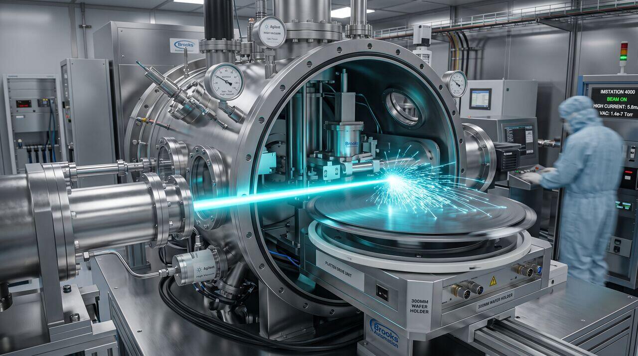
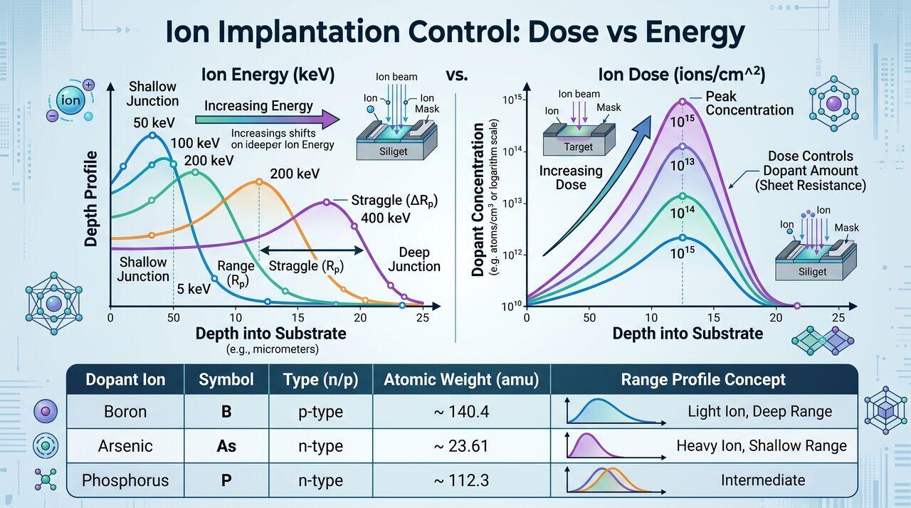
Ion implantation offers two independently controlled parameters that thermal diffusion could never provide:
- Ion Energy (E, measured in electron-volts - or ):
- Controls the depth profile of the implanted dopants. Higher acceleration voltages push ions deeper into the substrate ( depth; depth).
- Ion Dose (, measured in ):
- Controls the total concentration of dopant atoms. Integrates the total ion current delivered to the wafer over time.
- Ranging from low-dose threshold adjusts () to ultra-high dose source/drain implants ().
03The Need for Thermal Annealing
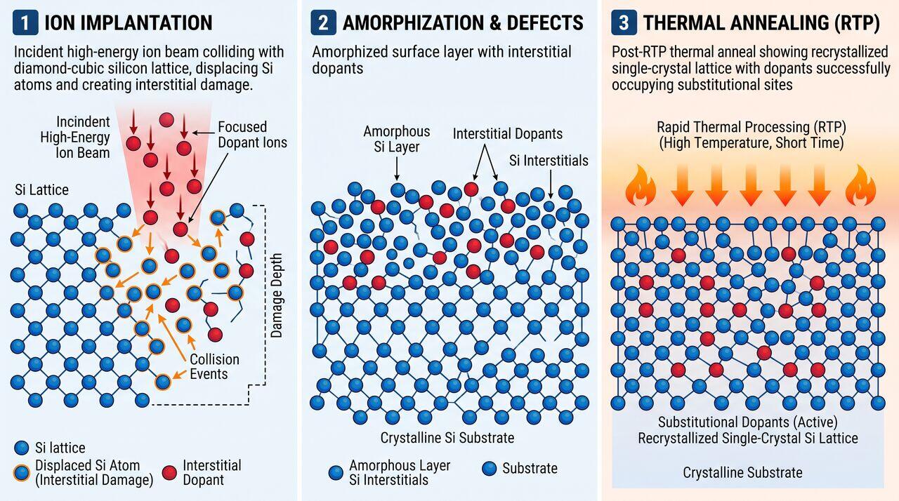
When high-energy ions impact the monocrystalline silicon substrate, they collide violently with silicon atoms, knocking them out of their lattice sites and destroying the crystal structure, creating an amorphous damage layer. Furthermore, the implanted dopant atoms reside in non-electrical interstitial positions.
To restore device operation, the wafer must undergo Thermal Annealing (e.g., Rapid Thermal Processing - RTP or Laser Annealing):
Annealing achieves two critical goals:
- Lattice Damage Repair: Recrystallizes the amorphized silicon back into a defect-free single crystal via Solid-Phase Epitaxial Regrowth (SPER).
- Dopant Activation: Drives implanted dopant atoms onto substitutional lattice sites where their valence electrons can contribute to electrical conduction.
→Prerequisites & continue reading
Prerequisites: ["p01-t1.1-t1-quartzite-to-mg-si-fundamentals"]
Also in Topic 7.3, Ion Implantation & Thermal Annealing:
Tier 2 · Ion Implanter Tool Architecture & Rapid Thermal Anne…Tier 3 · Ion Channeling, Transient Enhanced Diffusion (TED) &…