01Stopping Power Theory & Ion Channeling Physics
As an energetic ion penetrates the target, it loses kinetic energy (E) per unit path length (x) through two distinct stopping mechanisms according to Lindhard-Scharff-Schiøtt (LSS) Theory:
- Nuclear Stopping (): Elastic billiard-ball collisions between the ion and silicon atomic nuclei. Dominates at low energy, causing heavy crystal lattice damage and atom displacement.
- Electronic Stopping (): Inelastic drag forces caused by interactions with the target's electron cloud. Dominates at high energy, slowing the ion without causing lattice damage.
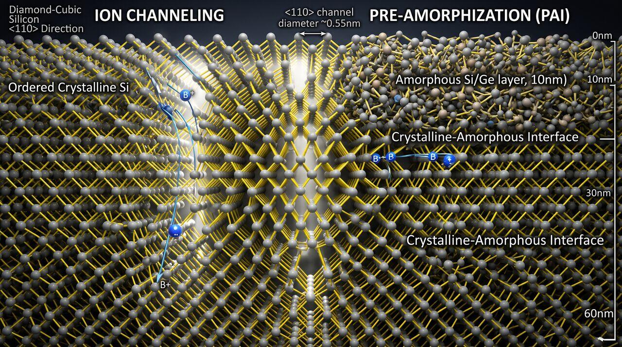
Ion Channeling:
When an ion beam is aligned along major open crystallographic directions of the diamond-cubic lattice (such as $\langle 110
angleor\langle 100
angle$), ions experience zero nuclear collisions and glide deep into the crystal via soft electronic drag, creating an unwanted long "tail" in the depth distribution profile!
Channeling Mitigation:
- Wafer Tilt: Tilting the wafer angle by off-axis breaks alignment with major crystal axes.
- Pre-Amorphization Implantation (PAI): Implanting heavy non-dopant ions (like Silicon or Germanium ) prior to boron implantation completely amorphizes the top silicon layer, converting it into a random glass structure where channeling is physically impossible.
02Transient Enhanced Diffusion (TED) Mechanics
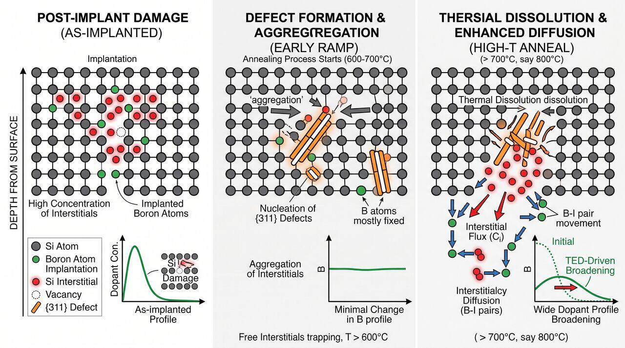
During thermal annealing, dopants like Boron diffuse orders of magnitude faster than predicted by equilibrium Fickian diffusion equations. This anomalous rapid movement is known as Transient Enhanced Diffusion (TED).
The {311} Defect Mechanism:
- Implantation generates a large excess population of self-interstitial silicon atoms ().
- Upon heating, these interstitials aggregate into planar rod-like defects and dislocation loops.
- As defects dissolve between and , they emit a massive flux of free silicon interstitials.
- Boron diffuses almost exclusively via an interstitialcy mechanism $(\text{B} + \text{Si}_I
\rightleftharpoons \text{B}_I). The excess interstitial flux drives rapid anomalous boron diffusion until all\{311\}$ defects are fully annealed out!
03Ultra-Shallow Junction (USJ) Engineering Strategy
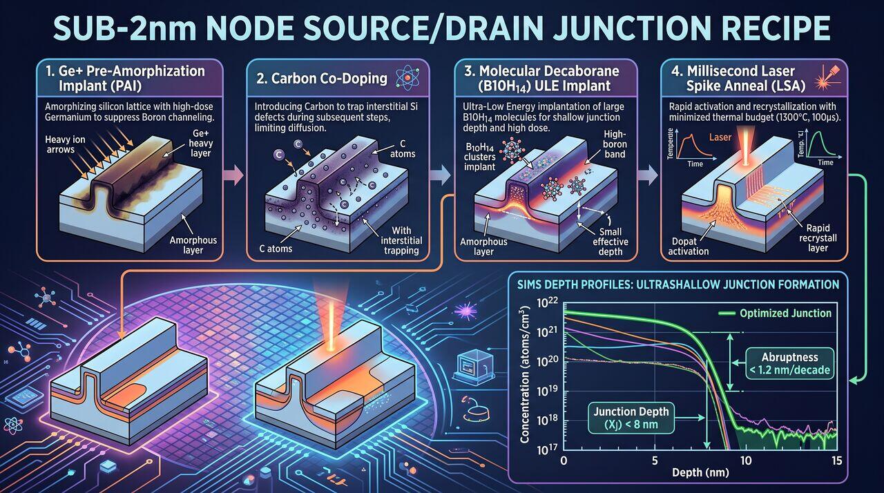
To suppress TED and achieve abrupt junctions:
- Carbon Co-Doping: Implanting Carbon () creates deep interstitial traps ($\text{C}_I + \text{Si}_I
\rightarrow \text{CSi}$ complexes), soaking up excess interstitials before they can pair with boron atoms.
- Cluster Ion Implantation: Utilizing large molecular ions like Decaborane () or Carborane (). Acceleration energy is divided among the 10 boron atoms, enabling effective sub-100 eV boron implantation with high beam current!
- Millisecond Laser Spike Annealing (LSA): Heating the surface to for recrystallizes the PAI layer and activates boron before defects have time to dissolve and emit interstitials, freezing the ultra-shallow profile in place.
→Prerequisites & continue reading
Prerequisites: ["p07-t7.3-t2-ion-implanter-hardware-beamline-spike-anneal-mechanics"]
Also in Topic 7.3, Ion Implantation & Thermal Annealing:
Tier 1 · Ion Implantation & Thermal Annealing Fundamentals…Tier 2 · Ion Implanter Tool Architecture & Rapid Thermal Anne…