01Tool Architecture & Reticle Enhancement Technologies (RET)
As process nodes scaled from 65 nm down to the 7 nm regime, basic Rule-Based OPC (applying fixed geometric rules) was replaced by Model-Based OPC (MB-OPC) and advanced Reticle Enhancement Technologies (RET).
1.1 Sub-Resolution Assist Features (SRAF)
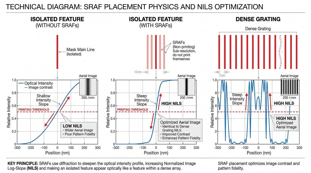
Isolated circuit lines lack the adjacent scattering neighbors present in dense line arrays, causing them to print with poor depth-of-focus (DOF). To fix this, OPC engines automatically insert Sub-Resolution Assist Features (SRAFs):
- SRAFs are extremely narrow parallel bars placed alongside main circuit features.
- They are sized below the printing resolution of the scanner optics, meaning they do not print on the wafer.
- However, their diffracted light constructively interferes with the main feature, restoring dense-like focus latitude and dramatically expanding the exposure Process Window.
02Photoresist Processing Mechanics & PEB Track Kinetics
The chemical conversion of a Chemically Amplified Resist (CAR) requires exquisite thermal and environmental control within the automated Coat/Develop Track tool:
2.1 Post-Exposure Bake (PEB) Thermal Uniformity
The Post-Exposure Bake (PEB) step is the most critical thermal process in lithography. During PEB (typically \(100-130^\circ\text{C}\) for 60 seconds), thermal energy drives acid-catalyzed de-protection.
- Sensitivity: A \(1.0^\circ\text{C}\) variation in PEB temperature across the bake plate can cause a 1 to 2 nm shift in printed feature CD.
- Specification: Modern track tools utilize multi-zone proximity bake plates controlled to within an extraordinary \(\pm 0.05^\circ\text{C}\) across the entire 300 mm wafer surface.

03Operational Defectivity & Process Window Optimization
3.1 Edge Placement Error (EPE)
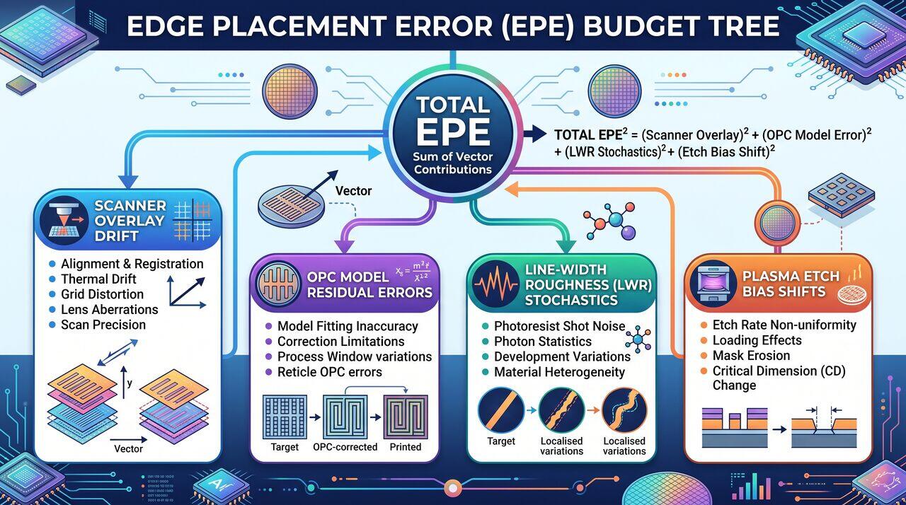
In advanced multi-patterning and EUV integration, the primary lithography yield metric is Edge Placement Error (EPE), defined as the total spatial mismatch between the intended physical edge of a feature and its actual printed location on wafer:
If EPE exceeds 25% of the feature pitch, catastrophic yield failures occur: either electrical shorts (bridging defects) or open circuits (line breakage).
04Media Companion Prompts
Media Prompt 1 (Photorealistic Render)
- Prompt: A detailed 3D render inside an automated photoresist track bake module. A 300mm silicon wafer rests on a high-precision multi-zone thermal bake plate, emitting subtle heat shimmering air currents. Precision robot handler arms with vacuum end-effectors position the wafer under clean laminar airflow. Industrial semiconductor automation aesthetic, cleanroom lighting, 8k.
Media Prompt 2 (Technical Vector Diagram)
- Prompt: A technical vector diagram illustrating Sub-Resolution Assist Feature (SRAF) placement physics. Shows an isolated main line without SRAFs exhibiting a narrow, shallow optical intensity slope versus an isolated main line flanked by non-printing SRAFs displaying a steep Normalized Image Log-Slope (NILS) identical to dense gratings.
Media Prompt 3 (Educational Infographic)
- Prompt: An educational infographic mapping the Edge Placement Error (EPE) budget tree. Shows how total EPE is calculated by summing vector contributions from Scanner Overlay Drift, OPC Model Residual Errors, Line-Width Roughness (LWR) stochastics, and Plasma Etch Bias shifts.
→Prerequisites & continue reading
Prerequisites: ["p05-t5.3-t1-opc-computational-lithography-resist-fundamentals"]
Also in Topic 5.3, Computational Lithography & OPC:
Tier 1 · OPC, Computational Lithography & Photoresist Fundame…Tier 3 · Inverse Lithography (ILT), CAR Acid Blur & Photon St…