01Introduction & The "What You See Is NOT What You Print" Paradox
In the early days of semiconductor manufacturing, the circuit patterns drawn by chip designers on layout CAD tools matched the physical features printed on silicon wafers almost perfectly. However, as transistor feature sizes scaled below the wavelength of exposure light (e.g., printing 32 nm lines with a 193 nm light source), optical diffraction, lens aberration, and resist diffusion severely distorted the projected image.
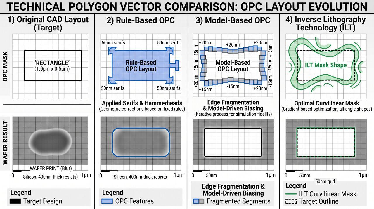
If an uncorrected rectangular circuit layout is placed on a modern photomask, optical diffraction causes line ends to pull back (line-end shortening), sharp 90-degree corners to round off (corner rounding), and isolated lines to print at a completely different width than dense lines (pitch-dependent bias).
Optical Proximity Correction (OPC) is the core discipline of computational lithography that mathematically modifies the shapes on a photomask, adding tiny serifs, hammerheads, and bias adjustments, so that after light diffracted through the optics, the final printed pattern on the wafer perfectly matches the designer's original rectangular intent.
02Key Process Inputs & Outputs
- Inputs:
- Target GDSII / OASIS Layout: Geometric circuit pattern files generated by Electronic Design Automation (EDA) physical design tools.
- Lithography Simulation Models: Calibrated mathematical models describing scanner optical diffraction, illumination pupil shape, and photoresist chemical response.
- Outputs:
- Corrected Mask Data Prep (MDP): Heavily modified polygon geometry featuring sub-resolution assist features (SRAF), serifs, and biased line edges ready for electron-beam mask writing.
03Photoresist Fundamentals: Positive vs. Negative & CAR Mechanics
To capture the corrected light image, the wafer is coated with a thin polymer film called a photoresist.
Chemically Amplified Resists (CAR)
Modern DUV and EUV lithography rely on Chemically Amplified Resists (CAR). A CAR film consists of three main components:
- Base Polymer: Protected by chemical blocking groups that make it insoluble in aqueous developer.
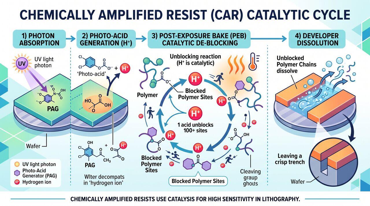
- Photo-Acid Generator (PAG): A photo-sensitive molecule that cleaves upon absorbing a photon, releasing a strong acid (\(\text{H}^+\)).
- Cross-Linker / De-blocking Agent: During Post-Exposure Bake (PEB), a single photo-generated acid molecule acts as a catalyst, triggering hundreds of chemical de-protection reactions (chemical amplification), making the exposed polymer highly soluble while regenerating the acid.
04Media Companion Prompts
Media Prompt 1 (Photorealistic Render)
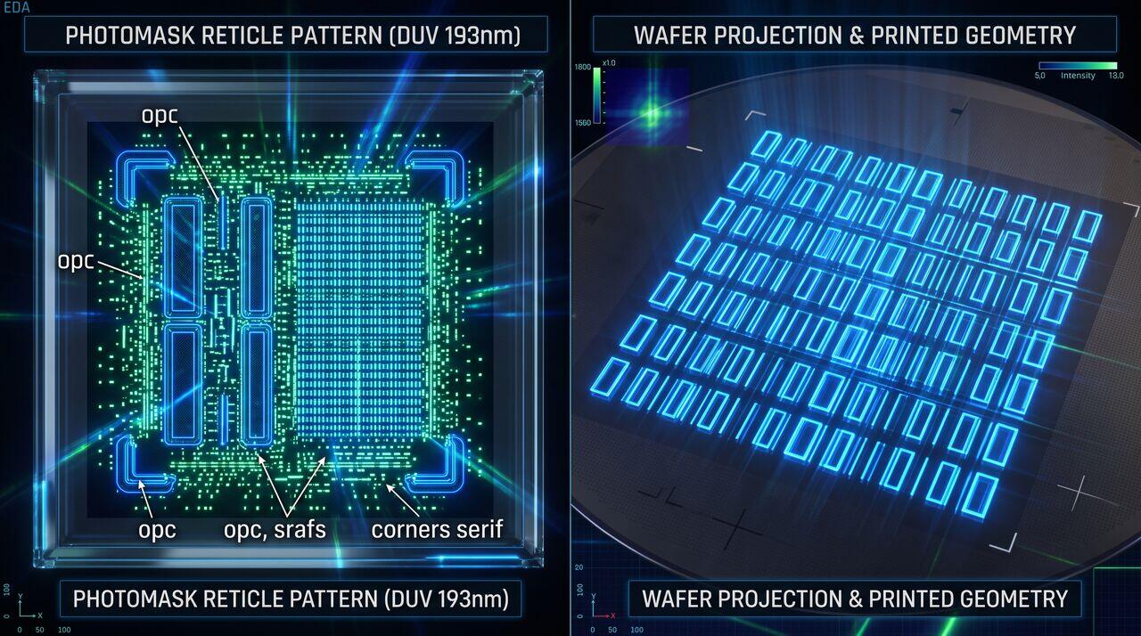
- Prompt: A high-contrast side-by-side visualization of a semiconductor photomask reticle pattern next to its illuminated projection on a silicon wafer. Shows intricate sub-resolution assist features (SRAFs) and corner serifs glowing on the mask, transforming into perfectly crisp rectangular transistor gate geometries on the wafer below. Photorealistic EDA software simulation aesthetic, glowing blue and green light vectors.
Media Prompt 2 (Technical Vector Diagram)
- Prompt: A technical polygon vector comparison showing OPC layout evolution: 1) Original CAD Layout (simple rectangle), 2) Rule-Based OPC (addition of corner serifs and hammerheads), 3) Model-Based OPC (fragmented line edges with biased segments), and 4) Inverse Lithography Technology (ILT, curvilinear organic-looking mask shapes).
Media Prompt 3 (Educational Infographic)
- Prompt: An educational infographic detailing the Chemically Amplified Resist (CAR) catalytic cycle. Shows a 4-step sequence: 1) Photon Absorption by PAG molecule, 2) Photo-acid generation (H+), 3) Post-Exposure Bake (PEB) catalytic de-blocking reaction (1 acid unblocking 100+ polymer sites), 4) Developer dissolution of unblocked polymer chains leaving a crisp trench.
→Prerequisites & continue reading
Prerequisites: ["p05-t5.1-t1-duv-immersion-193i-lithography-fundamentals"]
Also in Topic 5.3, Computational Lithography & OPC:
Tier 2 · OPC Reticle Enhancement, Model Calibration & CAR Pro…Tier 3 · Inverse Lithography (ILT), CAR Acid Blur & Photon St…