01Hardware Architecture & Tool Mechanics
Fabricating sub-20nm Dual-Damascene copper interconnects requires a closely integrated equipment train comprising three core unit operations:
- Pre-Treatment & Pore Sealing Modules: Plasma or ALD chambers dedicated to sealing open pores on etched Low-k trench sidewalls.
- Physical Vapor Deposition (PVD) Cluster Tool: Ultra-high vacuum (UHV) chambers for depositing ultra-thin conformal diffusion barriers (TaN/Ta) and copper seed layers.
- Electrochemical Plating (ECP) Module: Single-wafer wet fountain plating cells utilizing organic additive chemistry to achieve bottom-up "superfilling."
A. PVD Barrier/Seed Cluster Chamber
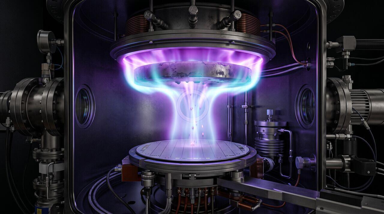
Modern PVD barrier tools utilize Ionized PVD (iPVD) or Self-Sustaining Ion Metal Plasma (SSIMP). High-density DC magnetron sputtering produces metal atoms that pass through an inductively coupled plasma (ICP) region, ionizing of the sputtered Ta/TaN or Cu atoms. An applied RF bias on the wafer chuck accelerates these metal ions vertically into high-aspect-ratio trenches and vias, ensuring adequate sidewall and bottom coverage without over-depositing at the trench overhang.
B. ECP Fountain Cell Hardware
The ECP cell holds the wafer face-down using a specialized contact ring with elastomeric seals and flexible electrical contact pins that supply cathode bias to the conductive PVD Cu seed layer. Electrolyte solution () is pumped upward through a diffuser plate to form a stable, bubble-free fountain meniscus against the rotating wafer ().
02Low-k Pore Sealing Mechanics
As interlayer dielectrics (ILD) transition to ultra-low-k formulations (k < 2.4), open nano-porosity ( pore diameter) is introduced into the matrix to lower the bulk dielectric constant. However, plasma etching exposes open pores along trench sidewalls. If unsealed, subsequent PVD barrier metal or precursor gases can penetrate into the bulk dielectric, creating metallic shunts, lowering breakdown voltage (), and dramatically increasing .
To prevent this, Pore Sealing must be executed prior to barrier deposition:
- Plasma-Assisted Stuffing: Brief exposure to , , or plasmas creates a dense, highly cross-linked amorphous skin ( thick) that seals open surface pores.
- Self-Assembled Monolayers (SAM) / ALD Sealing: Deposition of organic silane monolayers or ultra-thin ALD () to physically plug surface pore throats without adding significant capacitive thickness.
03PVD TaN/Ta Barrier & Copper Seed Deposition
Copper diffuses rapidly through silicon and dielectrics under thermal and electrical stress, acting as a deep-level trap that degrades device performance. A bi-layer Tantalum Nitride / Tantalum (TaN/Ta) diffusion barrier is mandatory:
- TaN Layer (): Deposited directly onto the Low-k sidewall via reactive PVD (Ta target + gas). Amorphous TaN provides exceptional thermal stability and prevents copper grain-boundary diffusion.
- Ta Layer (): Deposited over TaN. Ta grows in the low-resistivity alpha-phase (), providing an ideal crystallographic template for adhering and orienting the subsequent copper seed layer.
- PVD Copper Seed (): Provides the electrical conductivity required to carry plating current across the 300mm wafer during initial ECP immersion.
04Electrochemical Plating (ECP) & Superfilling Kinetics
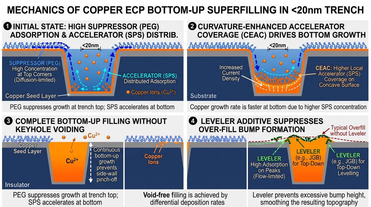
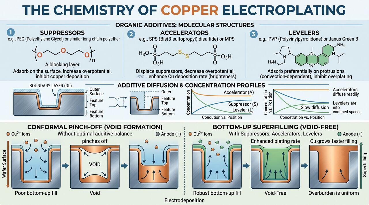
Traditional electroplating deposits metal uniformly over all surfaces, which causes high-aspect-ratio features to pinch off at the top opening, creating large internal keyhole voids. To achieve bottom-up superfilling (void-free fill), ECP baths rely on three critical organic additives:
| Additive | Molecular Weight | Diffusion Rate | Primary Function & Mechanism |
|---|---|---|---|
| Suppressor (PEG) | High () | Slow | Polyethylene glycol molecules adsorb onto top corners and upper sidewalls in the presence of ions, forming a resistive barrier that retards local copper deposition rate. |
| Accelerator (SPS) | Low () | Fast | Bis(3-sulfopropyl)disulfide accumulates at via/trench bottoms. As the feature area shrinks, local SPS concentration increases, displacing suppressors and dramatically accelerating copper growth. |
| Leveler (Janus Green B) | High, Positively Charged | Mass-Transfer Limited | Strong cationic molecules migrate preferentially to high-electric-field protrusions and top corners, preventing over-plating ("bump" formation) after features are filled. |
05Summary & Key Takeaways
- Pore Sealing prevents PVD barrier penetration and dielectric degradation in ultra-low-k (k < 2.4) porous films.
- Bi-layer TaN/Ta PVD Barriers prevent copper migration (TaN) and provide adhesion ().
- Ionized PVD (iPVD) directs metal ions vertically into high-aspect-ratio features using wafer chuck bias.
- ECP Superfilling is governed by additive kinetics: Suppressors retard top deposition, while Accelerators accumulate at trench bottoms to drive bottom-up, void-free copper growth.
→Prerequisites & continue reading
Prerequisites: ["p08-t8.1-t1-beol-dual-damascene-low-k-fundamentals.md"]
Also in Topic 8.1, BEOL Metallization, Dual Damascene & Low-k:
Tier 1 · BEOL Metallization, Dual-Damascene & Low-k Dielectri…Tier 3 · Electromigration, RC Delay & Ultra-Low-k Physics…