01High-Level Purpose & Physical Motivation
In modern integrated circuits, fabricating high-performance transistors in the Front-End-of-Line (FEOL) represents only half the challenge. To form functional microprocessors, graphics processors, and memory arrays, billions of isolated transistors must be interconnected through a complex, multi-level network of microscopic metal wires. This complex interconnect hierarchy is fabricated during the Back-End-of-Line (BEOL) phase.
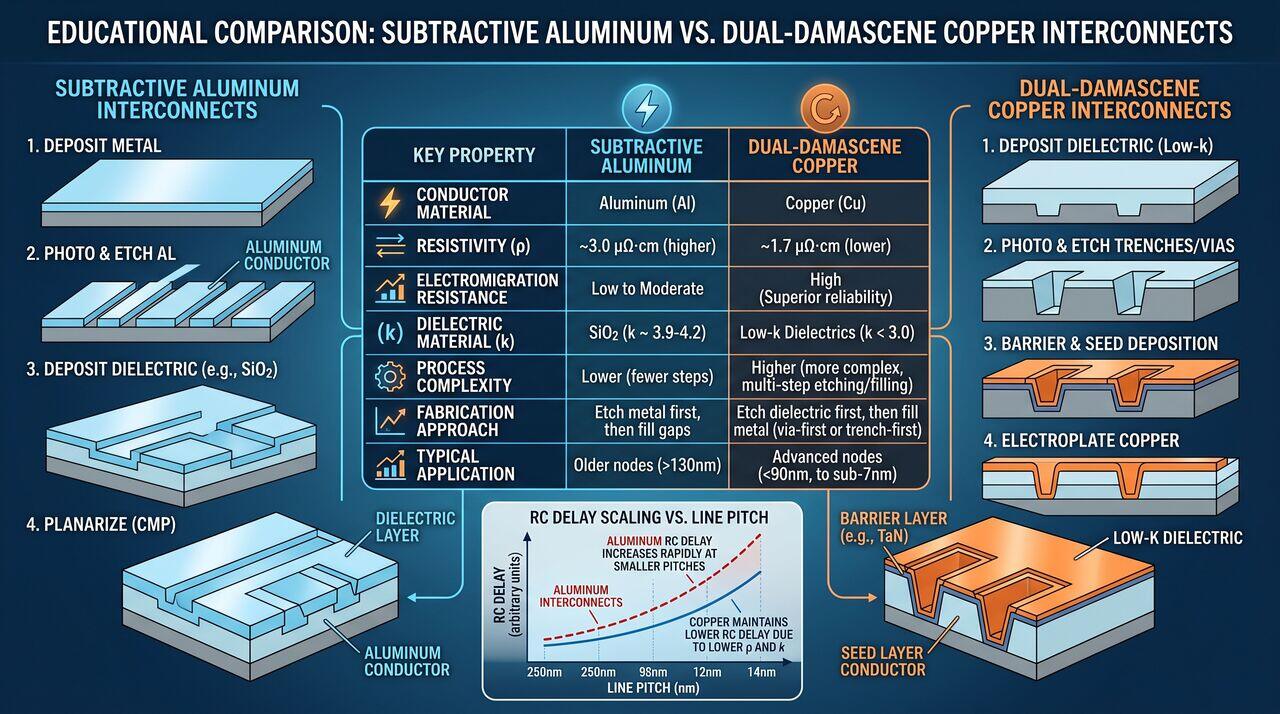
Historically, BEOL interconnects were built using aluminum (Al) patterned via subtractive reactive ion etching (RIE) with silicon dioxide (, ) as the insulating dielectric. However, as transistor scaling pushed feature sizes below the node, two critical physical bottlenecks emerged:
- RC Signal Delay: The propagation delay () along interconnect lines began to dominate overall gate switching delay.
- Electromigration (EM): High current densities in narrow aluminum lines caused momentum transfer from moving electrons to metal ions, driving void formation and open-circuit failures.
To overcome these physical limitations, the semiconductor industry transitioned to copper (Cu) interconnects starting at the node. Copper provides a lower electrical resistivity ( vs. ) and significantly higher electromigration resistance. However, copper poses a fundamental fabrication paradox: copper cannot be easily etched using conventional subtractive plasma etching because copper-halogen reaction byproducts (such as CuCl) have extremely low volatility at standard processing temperatures.
To solve this, IBM pioneered the Damascene process architecture, where dielectrics are etched first to create trenches and vias, followed by blanket copper deposition and Chemical Mechanical Planarization (CMP). Concurrently, dielectrics were replaced by Low-k and Ultra-Low-k (ULK) materials (k < 2.7) to minimize line-to-line capacitive coupling (C).
02Key Inputs, Outputs & Process Flow
Key Inputs
- Substrate: Wafer exiting Middle-End-of-Line (MEOL) with contact silicide pads (NiSi, ) or preceding lower-level metal layer ().
- Interlayer Dielectric (ILD): Carbon-doped oxide (SiCOH) or porous organosilicate glass (OSG).
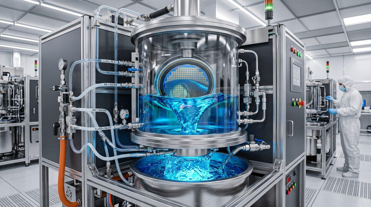
- Metallization Precursors: Copper sulfate electroplating baths (), PVD Tantalum/Tantalum Nitride (Ta/TaN) barrier targets, and PVD Copper seed targets.
Key Outputs
- Multi-Level Interconnect Architecture: Highly uniform, void-free copper wires and vertical vias insulated by mechanically stable Low-k dielectrics, spanning 10 to 15 metal layers ( through ).
03The Dual-Damascene Process Schemes
Unlike Single-Damascene, which fabricates vias and trenches in separate deposition, etch, and CMP cycles, Dual-Damascene forms both the vertical via and the horizontal wire trench in a single dielectric stack before executing a single copper electroplating and CMP sequence. This reduces processing steps, lowers manufacturing cost, and eliminates one resistive interface per layer.
There are two primary Dual-Damascene integration schemes:
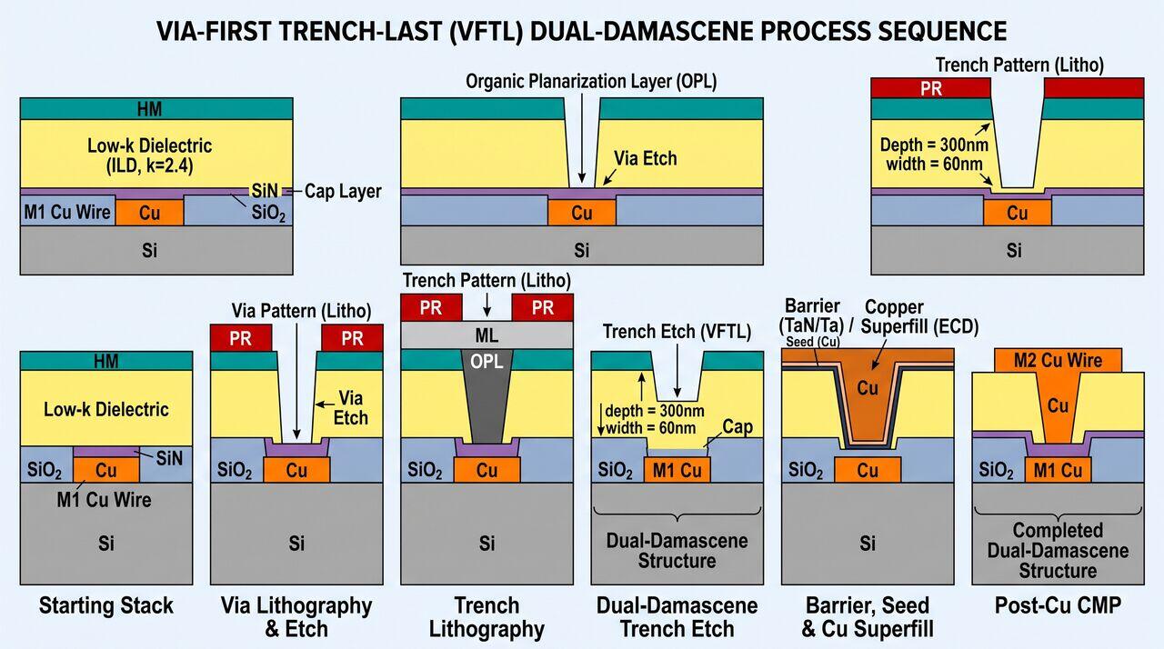
A. Via-First Trench-Last (VFTL)
- ILD Deposition: Blanket PECVD deposition of Low-k dielectric and cap layers.
- Via Lithography & Etch: Via pattern exposed and etched completely through the ILD down to the lower metal cap.
- Trench Lithography: Photoresist applied, filling the bottom of the via (or using a sacrificial organic planarization layer, OPL). The wire trench pattern is exposed.
- Trench Etch: Dielectric etched to the targeted trench depth while protecting the via floor.
- Cap Etch: Bottom dielectric cap removed to expose the underlying metal pad.
B. Trench-First Via-Last (TFVL)
- Trench Lithography & Partial Etch: Trench pattern etched partially into the upper region of the ILD.
- Via Lithography & Etch: Via pattern exposed inside the trench and etched down through the remaining ILD thickness to the lower metal layer.
Industry Standard: Via-First Trench-Last (VFTL) is the dominant industry standard due to wider lithographic focus margins and superior via floor depth control.
04Conceptual Analogy
Think of building a traditional brick house versus pouring a concrete structure with pre-cast molds:
- Subtractive Etching (Aluminum): Laying a solid sheet of metal across the entire floor, painting lines where you want wires, and using acid to dissolve away all the unwanted metal, leaving behind free-standing wires that you then try to pack around with insulation.
- Dual-Damascene (Copper): Carving precise channels and vertical holes into a solid block of hard foam (dielectric insulation), lining the channels with thin non-stick plastic wrap (diffusion barrier), pouring liquid copper into all channels until overfilled, and scraping off the excess metal with a flat trowel (CMP) to leave smooth, perfectly flush wires embedded inside the foam.
05Summary & Key Takeaways
- BEOL connects FEOL transistors into functional circuits using multi-level metal wires and vertical vias.
- Copper replaced aluminum due to lower electrical resistivity and superior electromigration resistance.
- Dual-Damascene is mandatory for copper because copper cannot be cleanly etched using subtractive halogen plasma etching.
- Low-k Dielectrics (SiCOH, k < 2.7) replace () to minimize RC signal propagation delay and line-to-line cross-talk capacitance.
→Prerequisites & continue reading
Prerequisites: ["p03-t3.2-t1-copper-damascene-barrier-cmp-fundamentals.md", "p07-t7.1-t1-thermal-oxidation-deal-grove-fundamentals.md"]
Also in Topic 8.1, BEOL Metallization, Dual Damascene & Low-k:
Tier 2 · Copper Electroplating, PVD Barrier & Pore Sealing Me…Tier 3 · Electromigration, RC Delay & Ultra-Low-k Physics…