01Mathematical & Kinetic Foundations of RC Scaling
As semiconductor interconnect pitches scale down into the sub-30nm regime, interconnect propagation delay replaces transistor gate delay as the primary bottleneck in digital circuit timing. The total signal delay () of an interconnect line of length L, wire width w, height h, line spacing s, and metal resistivity embedded in a dielectric of permittivity is expressed by the distributed RC model:
Where:
- R: Line resistance ()
- C: Total line-to-line and line-to-ground capacitance (F)
- : Temperature-dependent copper resistivity ()
- k: Relative dielectric constant of interlayer insulator
- : Interlayer dielectric thickness
Resistivity Size Effect (Fuchs-Sondheimer & Mayadas-Shatzkes Models)
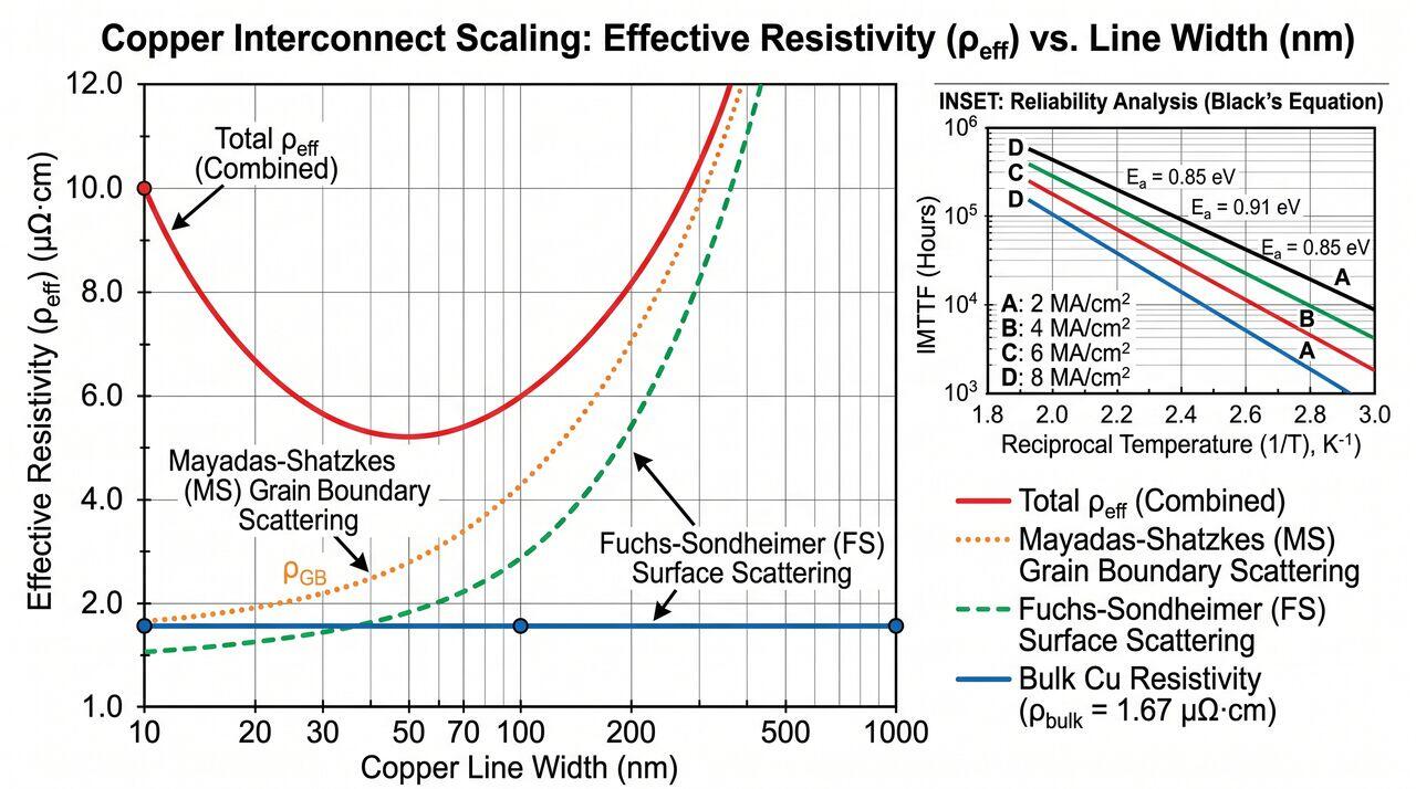
As trench dimensions approach the mean free path of conduction electrons in bulk copper ( at ), bulk resistivity assumptions fail. The effective resistivity () increases sharply due to two quantum-electron scattering mechanisms:
- Surface Specular Scattering (Fuchs-Sondheimer Model):
Where p is the specularity parameter ( for specular reflection, for diffuse scattering) and d is wire width.
- Grain Boundary Scattering (Mayadas-Shatzkes Model):
Where is the average copper grain size and is the grain-boundary reflection coefficient (0.2-0.5).
02Electromigration (EM) Physics & Kinetic Degradation
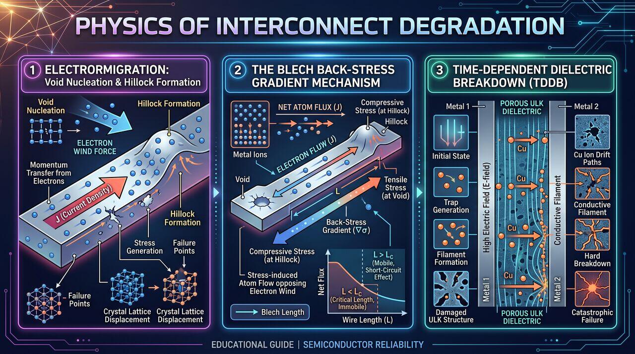
Electromigration is the transport of material caused by the gradual movement of metal ions in a conductor due to the momentum transfer between conducting electrons and the diffusing metal lattice. The net atomic flux () under an applied current density is governed by:
Where:
- : Atomic concentration of metal ions
- : Effective diffusion coefficient along dominant fast diffusion paths
- : Effective charge of metal ions (accounting for wind force of electrons)
- : Thermal energy
Black's Equation for Mean Time to Failure (MTTF)
Reliability lifespan under high current stress is predicted using Black's empirical equation:
Where:
- A: Cross-sectional area factor
- j: Current density ()
- n: Current density exponent ()
- : Activation energy for metal self-diffusion (eV)
In copper dual-damascene lines, diffusion occurs primarily along the Copper/Cap-Layer Interface (), rather than through bulk grains (). Implementing cobalt (Co) or ruthenium (Ru) cap layers increases activation energy to , extending MTTF by over .
The Blech Critical Length Effect
At short interconnect lengths (), electromigration is completely arrested by the buildup of a mechanical back-stress gradient (). The Blech Condition defines the threshold product of current density and length below which electromigration failure will never occur:
Where is atomic volume and is the maximum yield stress of the dielectric/barrier encapsulation.
03Ultra-Low-k (ULK) Physics & TDDB Reliability
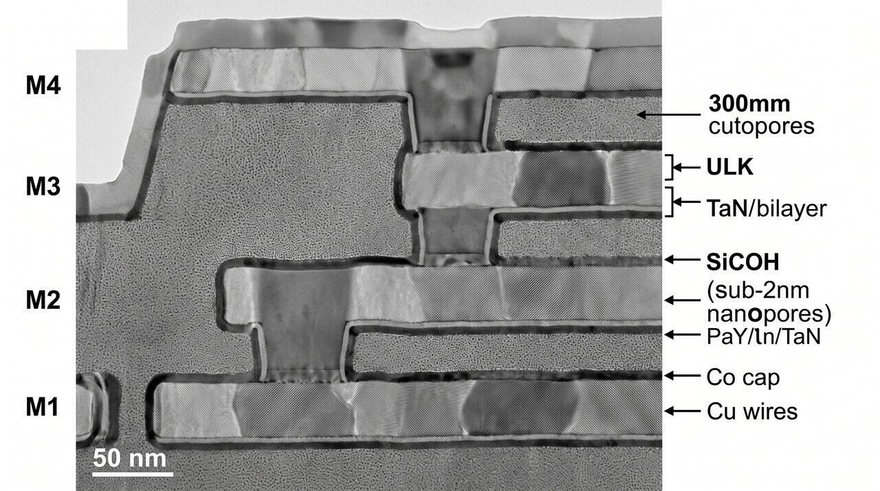
To push dielectric constants below , organosilicate glass (SiCOH) is engineered with nanometer-scale pores filled with air (). However, lowering k introduces critical reliability trade-offs:
- Mechanical Weakening: Bulk modulus (E) drops exponentially with porosity P:
- Time-Dependent Dielectric Breakdown (TDDB): Under high electric fields (), Cu ions injected across thin barriers degrade the dielectric lattice. Life expectancy is modeled using the E-model:
04Summary & Key Takeaways
- RC Delay scales non-linearly at sub-30nm dimensions due to Fuchs-Sondheimer surface and Mayadas-Shatzkes grain boundary electron scattering.
- Electromigration is driven by electron wind momentum transfer; diffusion along the interface dominates failure kinetics.
- Black's Equation models MTTF as a function of current density (j) and activation energy ().
- Blech Effect provides absolute electromigration immunity for short wire segments where back-stress balances electron wind forces ().
- Ultra-Low-k films (k < 2.2) trade mechanical strength () and TDDB margin for reduced line-to-line capacitance.
→Prerequisites & continue reading
Prerequisites: ["p08-t8.1-t2-copper-electroplating-pvd-barrier-pore-sealing-mechanics.md"]
Also in Topic 8.1, BEOL Metallization, Dual Damascene & Low-k:
Tier 1 · BEOL Metallization, Dual-Damascene & Low-k Dielectri…Tier 2 · Copper Electroplating, PVD Barrier & Pore Sealing Me…