01Hardware Architecture & Tool Integration
Direct Copper Hybrid Bonding execution requires an integrated equipment suite operating in ultra-clean environments:
- High-Precision CMP & Surface Profilometry Cluster: Chemical Mechanical Polishing tools engineered for sub-nanometer topography control and chemical pad recessing.
- Plasma Surface Activation & DI Water Scrubbing Module: Atmospheric or vacuum plasma chambers () integrated with high-pressure megasonic water scrubbers.
- High-Speed Optical Alignment & Bonding Cluster: Sub-100nm precision optical flip-chip die-to-wafer (D2W) or wafer-to-wafer (W2W) bonders.
- Vertical Batch Thermal Annealing Furnace: Cleanroom furnaces supporting controlled-environment nitrogen annealing ().
02Extreme Particle Cleanliness & Void Physics
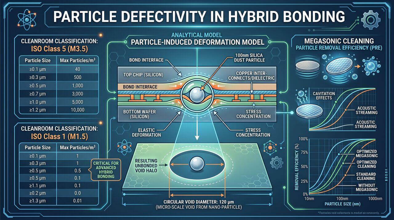
In conventional packaging, micro-bump solder can absorb and encapsulate airborne dust particles. In Direct Hybrid Bonding, a single particle as small as will create an unbonded void area over in diameter ( particle size) due to elastic bending of the surrounding wafer dielectric.
Cleanroom & Fluid Handling Protocols
- ISO Class 1 Environment: Optical bonding chambers operate under ISO Class 1 enclosures (< 10 particles per of air).
- Non-Contact Handling: End-effectors utilize Bernoulli or non-contact electrostatic gripping to prevent particle generation on wafer edges.
- Point-of-Use Megasonic Scrubbing: Prior to bonding, surfaces undergo high-speed megasonic DI water scrubbing combined with dilute ammonia () to achieve zero surface particle adders ( removal efficiency for particles ).

03Die-to-Wafer (D2W) vs. Wafer-to-Wafer (W2W) Mechanics
Hybrid bonding is executed using two primary mechanical integration approaches:
| Parameter | Wafer-to-Wafer (W2W) | Die-to-Wafer (D2W) |
|---|---|---|
| Throughput | Extremely High (100,000+ interconnects/min) | Moderate to High (1,000 - 5,000 UPH) |
| Die Size Flexibility | Identical die sizes required for top & bottom | Heterogeneous dies of varying sizes |
| KGD Support | Low (Known Good Die cannot be pre-screened) | High (Only Known Good Dies are placed on wafer) |
| Alignment Accuracy | Sub-100nm across entire 300mm wafer | Sub-200nm individual die placement |
| Primary Application | CMOS Image Sensors, 3D NAND, HBM4 Stacks | High-performance AI compute (CoWoS, SoIC) |
Die-to-Wafer Collective & Direct Placement
In D2W Direct Placement, singulated KGD chiplets are picked from dicing tape, visually aligned via high-magnification infrared/optical cameras, and placed individually onto the active base wafer. The bonder applies a light initial contact force (), triggering a spontaneous wave of intermolecular dielectric bonding that propagates across the chiplet interface in milliseconds.
04Sub-Nanometer Topography & Copper Recess Control
Achieving high-yield hybrid bonding requires ultra-rigorous control of surface topography prior to bonding.
The Chemical Recess Requirement
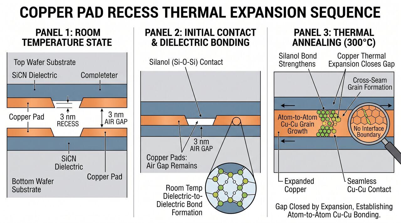
Because dielectric bonding occurs at room temperature while copper metallic bonding occurs during thermal annealing, the copper contact pads must be chemically recessed below the dielectric plane during CMP:
- If Recess is Too Shallow (): Copper expansion during annealing creates high localized stress that forces dielectric surfaces apart, causing interface delamination.
- If Recess is Too Deep (): Expanding copper fails to bridge the air gap during thermal annealing, leaving unbonded contact voids that cause open-circuit electrical failures.
05Summary & Key Takeaways
- Sub-100nm Particles cause massive unbonded void areas (), requiring ISO Class 1 cleanrooms and megasonic water scrubbing.
- Wafer-to-Wafer (W2W) provides maximum throughput for identical die dimensions (CIS, HBM4).
- Die-to-Wafer (D2W) enables Known-Good-Die (KGD) pre-screening and multi-node heterogeneous AI integration.
- Copper Pad Recess () via CMP is critical: balances room-temperature dielectric contact with thermal copper expansion welding.
→Prerequisites & continue reading
Prerequisites: ["p08-t8.3-t1-hybrid-bonding-chiplets-cowos-hbm4-fundamentals.md"]
Also in Topic 8.3, Hybrid Bonding & Chiplet Integration:
Tier 1 · Direct Copper Hybrid Bonding & Chiplet Integration: …Tier 3 · Surface Activation, Dislocation Interdiffusion & The…