01High-Level Purpose & Physical Motivation
For decades, performance gains in computer architecture were driven by Monolithic Integration, building an entire system-on-chip (SoC) on a single massive silicon die. However, as semiconductor fabrication approaches atomic physical limits, monolithic scaling has hit severe economic and yield barriers:
- The Reticle Limit & Yield Economics: Modern EUV photolithography tools have a maximum single-exposure reticle limit (). Fabricating ultra-large monolithic AI processors near this limit results in exponentially lower yield, as a single random crystal defect ruins the entire giant die.
- Heterogeneous Optimization: Different functional blocks thrive on different process nodes. SRAM cache and high-speed analog I/O do not scale efficiently at advanced sub-2nm nodes, making it wasteful to fabricate them on expensive leading-edge silicon.
To overcome monolithic limits, the industry has embraced Heterogeneous Integration (Chiplets), disaggregating a large SoC into smaller, high-yielding functional dies ("chiplets") and reconnecting them with ultra-high-density packaging.
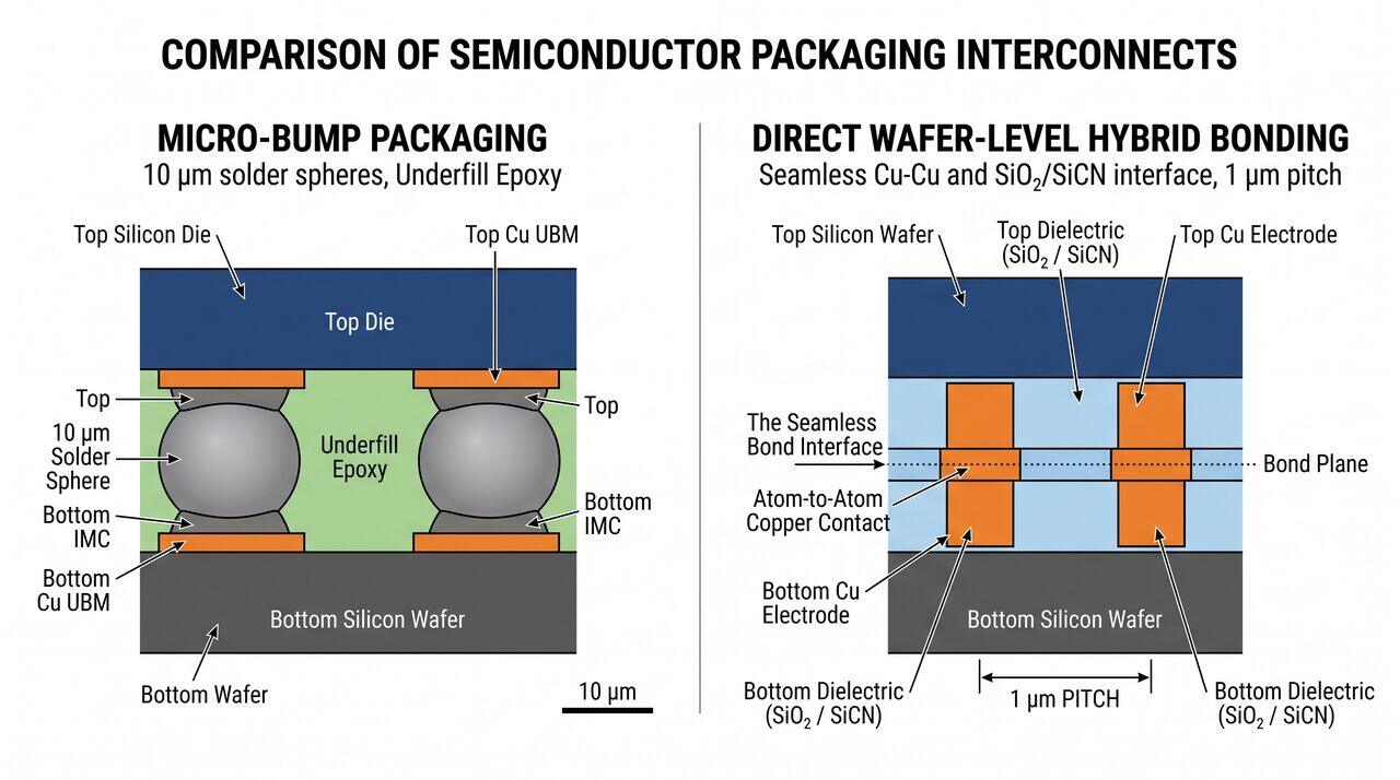
As interconnect pitch scaled below , traditional solder micro-bumps (C4, micro-bumps) failed due to solder bridging, high electrical resistance, and thermal dissipation bottlenecks. This triggered the transition to Direct Copper Hybrid Bonding (Cu-Cu DBI), which eliminates solder entirely by bonding dielectric-to-dielectric and copper-to-copper directly at atomic scales.
02Key Inputs, Outputs & Process Flow
Key Inputs
- Singulated Top Dies & Base Wafer: Highly planarized silicon wafers containing embedded, recessed copper contact pads surrounded by dielectric (, SiCN).
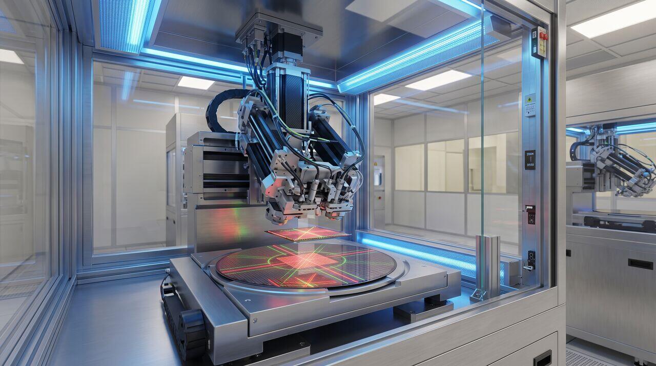
- Ultra-Clean Environment: ISO Class 1 cleanroom conditions to prevent sub-micron particle contamination at the bonding interface.
- Surface Activation Plasma: Nitrogen or oxygen plasma used to render dielectric surfaces highly hydrophilic.
Key Outputs
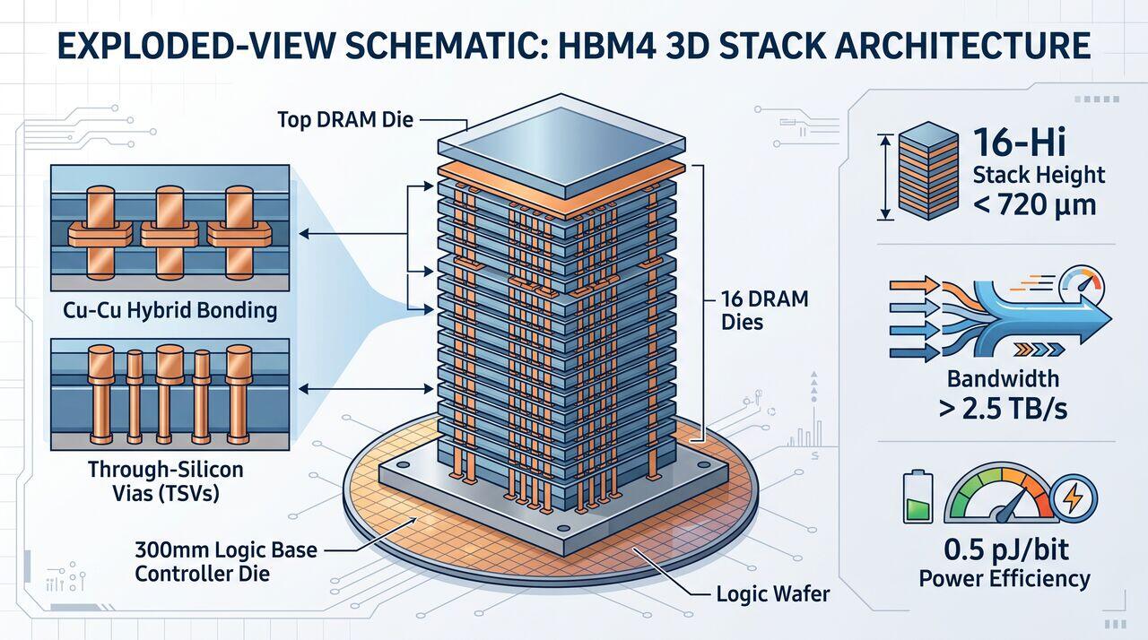
- Heterogeneous 2.5D/3D Integrated Module: Seamlessly bonded multi-die architecture (e.g., TSMC CoWoS, Intel Foveros Direct, HBM4 16-Hi stacks) featuring sub-micron interconnect pitch, low parasitic capacitance, and extreme bandwidth density ().
03Advanced Packaging Paradigms: 2.5D CoWoS vs. 3D Hybrid Bonding & HBM4
A. 2.5D Interposer Integration (e.g., TSMC CoWoS-S / CoWoS-L)
Chiplets are mounted side-by-side on a large silicon or organic interposer containing fine-pitch BEOL routing wires.
- CoWoS-S (Silicon Interposer): Uses a passive thinned silicon interposer with TSVs to connect AI logic dies to adjacent High Bandwidth Memory (HBM) stacks.
- CoWoS-L (Local Silicon Bridge): Replaces the massive silicon interposer with smaller silicon bridges embedded inside an organic substrate, reducing cost.
B. 3D Direct Hybrid Bonding (e.g., TSMC SoIC, Intel Foveros Direct)
Chiplets are stacked directly face-to-face on top of active logic wafers without interposers or solder bumps. Interconnect pitches drop below , yielding higher interconnect density and lower energy-per-bit transition compared to micro-bumps.
C. High Bandwidth Memory 4 (HBM4) Transition
HBM3e utilizes 12-Hi DRAM stacks joined by micro-bumps. In HBM4 (16-Hi stacks), micro-bump heights cause the stack to exceed standard package height limits. HBM4 transitions to Wafer-Level Hybrid Bonding, bonding 16 DRAM dies directly onto a custom logic base die, achieving unprecedented AI memory bandwidth ( per stack).
04Conceptual Analogy
Think of joining two wooden beams together:
- Micro-Bump Soldering: Putting thick globs of hot glue between two rough wooden posts. The glue holds them together, but leaves a wide gap, and if you press too hard, the glue squeezes out the sides and short-circuits neighboring connections.
- Direct Hybrid Bonding: Polishing the wooden beams so perfectly flat that their surfaces are smooth to an atomic level. When brought together at room temperature, the wood fibers spontaneously cling together without glue. Heating the joint causes copper pins embedded flush inside the wood to expand and weld into a single continuous solid beam.
05Summary & Key Takeaways
- Chiplet Architecture replaces monolithic SoCs to bypass reticle limits, boost manufacturing yields, and mix optimal process nodes.
- Direct Hybrid Bonding (Cu-Cu DBI) eliminates solder bumps, enabling sub-micron interconnect pitches ().
- The Hybrid Bonding Flow requires atomic-scale CMP planarization, plasma activation, room-temperature dielectric bonding, and thermal copper expansion annealing.
- Advanced AI Systems (NVIDIA Blackwell, AMD Instinct) rely on 2.5D CoWoS and 3D HBM4 hybrid bonding to deliver massive compute and memory bandwidth.
→Prerequisites & continue reading
Prerequisites: ["p08-t8.1-t1-beol-dual-damascene-low-k-fundamentals.md", "p08-t8.2-t1-tsv-wafer-thinning-bspdn-fundamentals.md"]
Also in Topic 8.3, Hybrid Bonding & Chiplet Integration:
Tier 2 · Cu-Cu Hybrid Bonding Cleanliness, Equipment & Die-to…Tier 3 · Surface Activation, Dislocation Interdiffusion & The…