01Thermodynamic Principles of Room-Temperature Dielectric Bonding
The initial step of direct hybrid bonding, spontaneous room-temperature dielectric-to-dielectric adhesion, is governed by surface energy chemistry and hydrogen bonding thermodynamics.
When an amorphous silicon dioxide () or silicon carbonitride (SiCN) surface is exposed to an oxygen or nitrogen plasma activation pretreatment, high-energy plasma ions break native siloxane bonds (Si-O-Si), creating a disordered, highly reactive surface layer ( deep). Subsequent deionized (DI) water rinsing terminates these open dangling bonds with hydrophilic silanol groups (Si-OH).
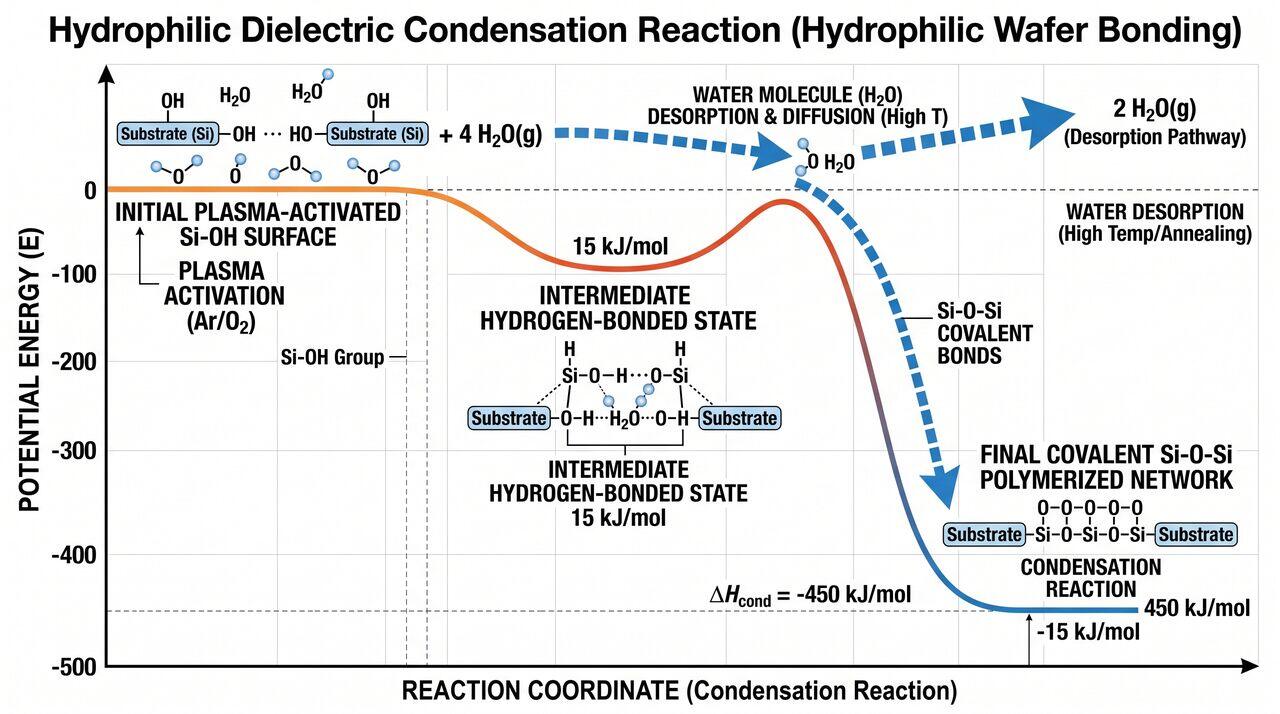
Hydrogen Bonding to Covalent Polymerization
When two activated wafers are brought into contact at , weak intermolecular hydrogen bonds form spontaneously across the silanol interface:
During thermal annealing (), water molecules desorb and diffuse away from the interface into the bulk dielectric matrix, driving a condensation polymerization reaction that converts weak hydrogen bonds into strong covalent siloxane bonds:
The surface work of adhesion () increases dramatically from at room temperature to (approaching the fracture toughness of bulk silicon) at temperatures above .
02Solid-State Metallic Cu-Cu Diffusion Kinetics
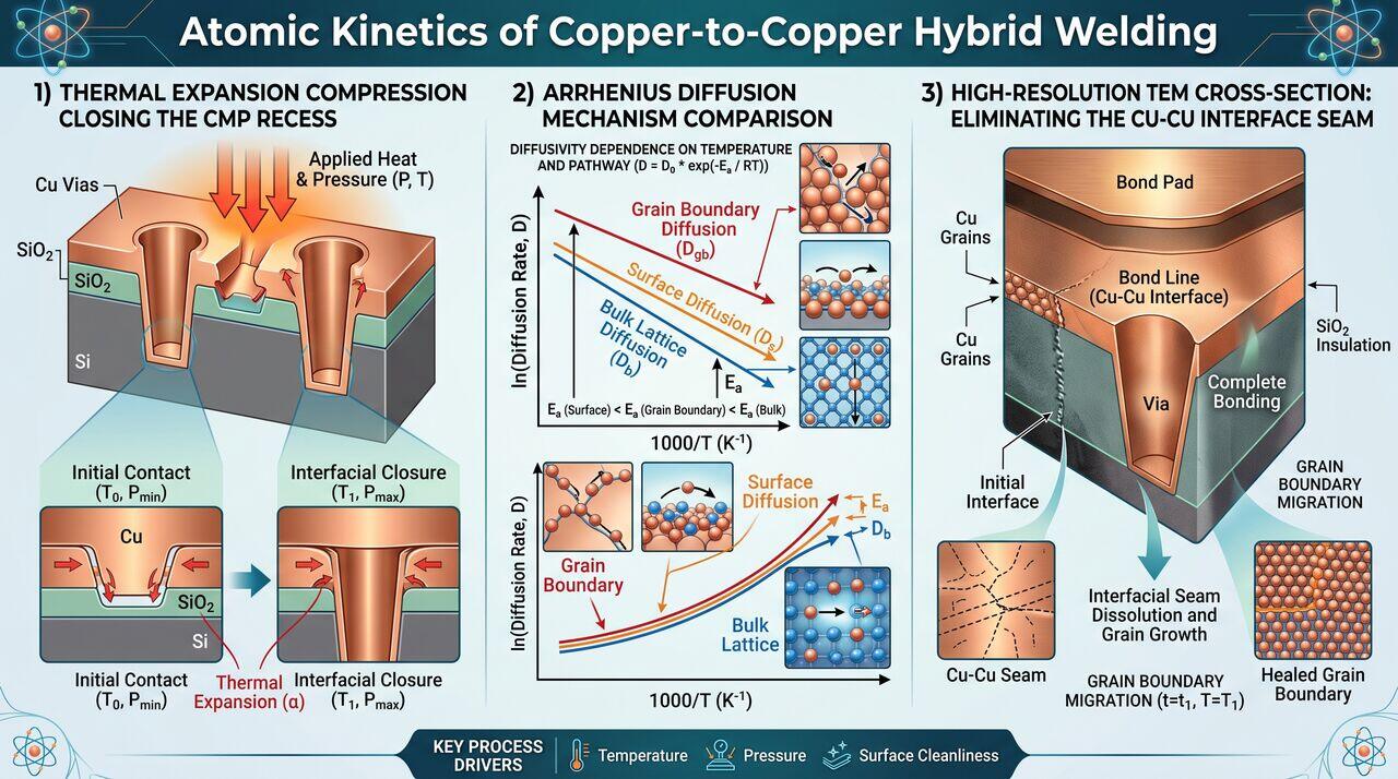
While the dielectric interface seals at , metallic copper-to-copper welding requires higher temperatures () to drive thermal expansion, close the CMP recess air gap, and initiate atom-to-atom interdiffusion.
Copper thermal expansion constraint builds up an internal compressive thermal stress ():
Once the expanding copper pads make physical contact across the interface, joint consolidation is driven by three coupled mass-transport mechanisms:
Interface Grain Boundary Migration & Seam Elimination
For complete electrical and mechanical consolidation, copper grain boundaries must migrate across the original bonding seam, eliminating the interface entirely. The grain boundary migration velocity under a driving stress is modeled by the Turnbull grain boundary mobility equation:
Where:
- : Grain boundary diffusion coefficient
- : Effective grain boundary width ()
- : Grain boundary energy
- : Average copper crystallographic grain radius
03Dislocation Creep & Low-Temperature Thermal Budget Physics
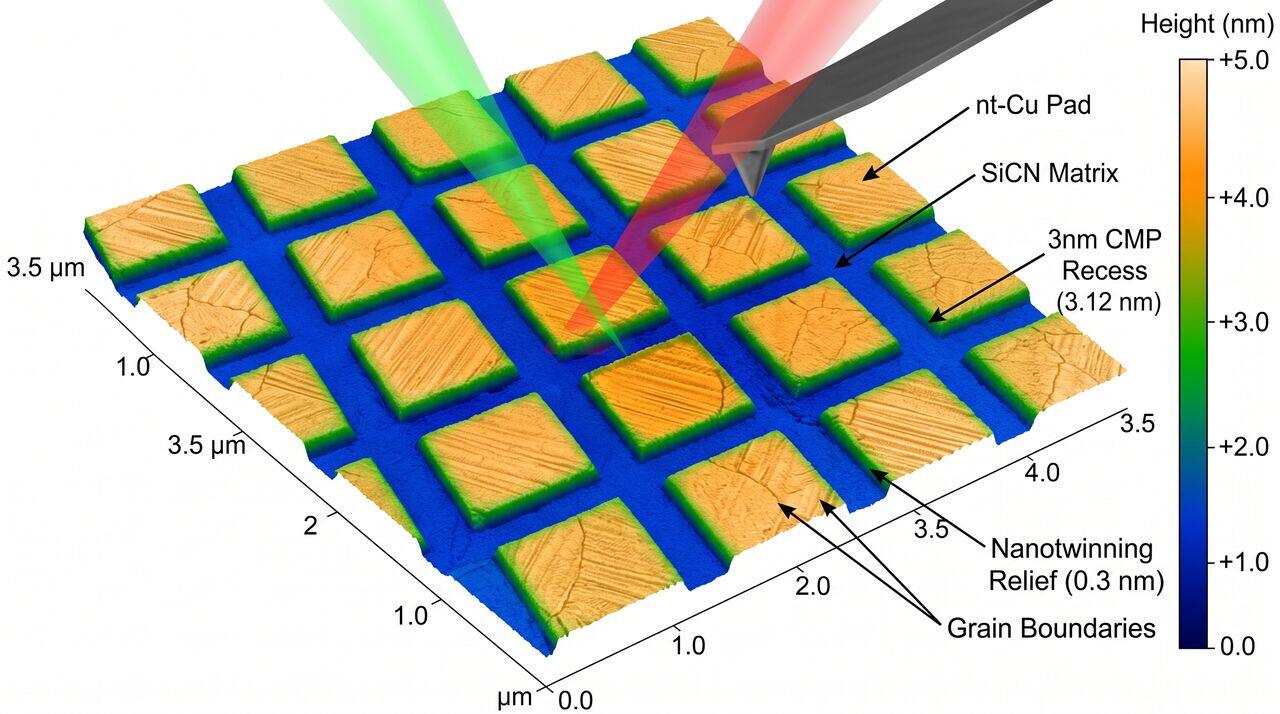
In advanced sub-2nm systems, high-temperature thermal annealing () damages delicate Front-End-of-Line (FEOL) ultrashallow junctions and extremely fragile porous Ultra-Low-k (ULK) dielectrics. To reduce bonding thermal budgets to , advanced hybrid bonding physics leverages two material innovations:
- Highly-Nanotwinned Copper (nt-Cu): Electrodeposited copper featuring high-density (111)-oriented preferred surface orientation and sub-50nm coherent twin boundaries. nt-Cu exhibits atomic surface diffusion rates up to faster than random polycrystalline copper, enabling robust atom-to-atom bonding at temperatures as low as .
- Dislocation Pipe Diffusion: High localized compressive stresses at expanding copper pad contact points activate dislocation multiplication and pipe diffusion (), enabling rapid low-temperature plastic flow that seals micro-voids without requiring long thermal hold times.
04Summary & Key Takeaways
- Plasma Activation breaks siloxane bonds, creating a high-energy hydrophilic silanol (Si-OH) surface layer.
- Condensation Polymerization converts weak hydrogen bonds into strong covalent siloxane bonds (), achieving bulk-silicon fracture toughness ().
- Thermal Expansion Pressure forces recessed copper pads into intimate contact during annealing.
- Grain Boundary Migration () eliminates the Cu-Cu bonding seam via combined surface, grain boundary, and lattice diffusion.
- Nanotwinned Copper (nt-Cu) enables low-temperature hybrid bonding () by accelerating surface diffusion by three orders of magnitude.
→Prerequisites & continue reading
Prerequisites: ["p08-t8.3-t2-cu-cu-hybrid-bonding-cleanliness-die-to-wafer-mechanics.md"]
Also in Topic 8.3, Hybrid Bonding & Chiplet Integration:
Tier 1 · Direct Copper Hybrid Bonding & Chiplet Integration: …Tier 2 · Cu-Cu Hybrid Bonding Cleanliness, Equipment & Die-to…