01Hardware Architecture & Process Train
Executing high-yield Through-Silicon Via (TSV) fabrication, extreme wafer thinning, and Backside Power Delivery Networks (BSPDN) requires a multi-equipment unit process train:
- High-Aspect-Ratio Etch Module: Deep Reactive Ion Etching (DRIE) Bosch process tools for etching 10:1 to 20:1 aspect ratio via holes.
- Vacuum Deposition & Electroplating Suite: SACVD/PECVD for conformal isolation liners, iPVD for Ti/Cu seed, and specialized periodic pulse reverse (PPR) electroplating cells.
- Temporary Wafer Bonding / Debonding System: High-precision adhesive spin-coaters and thermal/photonic debonding tools.
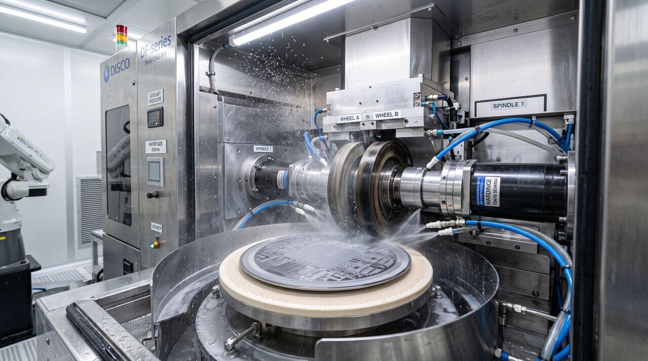
- Precision Backgrinding & Taiko Tools: Multi-spindle coarse/fine diamond-wheel grinding systems and chemical mechanical polishing (CMP) tools for TSV reveal.
02High-Aspect-Ratio TSV Filling Kinetics
Etching and filling a TSV ( diameter, depth, 10:1 aspect ratio) presents extreme mass-transfer challenges compared to shallow BEOL trenches:
A. Conformal Insulation Liner & Barrier Deposition
- Dielectric Isolation Liner (): Deposited via Sub-Atmospheric CVD (SACVD) using or Low-Temperature PECVD () to prevent electrical leakage into the bulk silicon substrate.
- Diffusion Barrier & Seed (): Ionized PVD (iPVD) sputtering of Titanium (Ti) or Tantalum (Ta) barrier and Copper (Cu) seed layer. High RF chuck bias is applied to drive metal ions deep into the cavity without pinching off the top entrance.
B. Specialized ECP Pulse Plating
Standard ECP DC current causes rapid top-opening pinch-off, leaving huge voids inside deep TSVs. To prevent this, Periodic Pulse Reverse (PPR) electroplating is employed:
- Forward Pulse (): Plating current applied to deposit copper along the via walls.
- Reverse Pulse (): Brief high-current anodic pulse that preferentially dissolves copper build-up from top entrance overhangs where electric fields concentrate.
- Organic Additive Dynamics: Extremely high concentrations of slow-diffusing Suppressors seal top openings, while strong Accelerators drive bottom-up growth.
03Wafer Thinning: Standard Carrier vs. DISCO Taiko Process
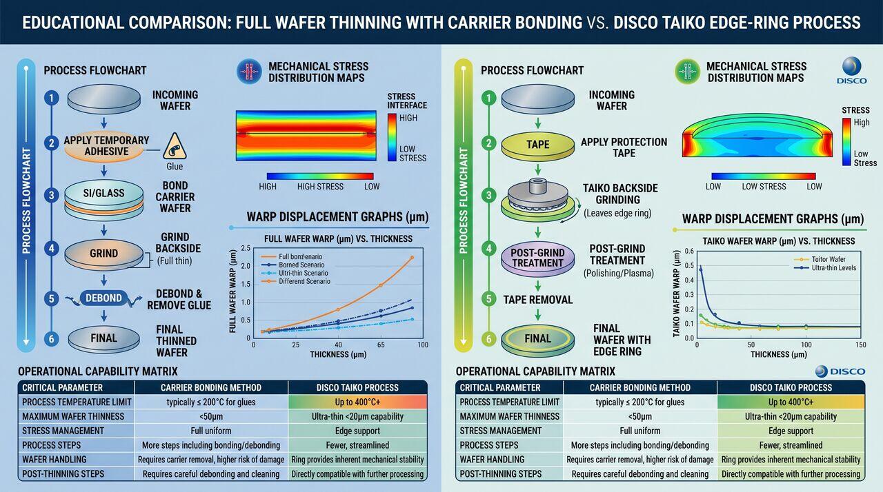
Thinning a silicon wafer from down to removes mechanical rigidity, causing extreme wafer warp and stress-induced fracturing. Two handling approaches are used:
A. Standard Temporary Carrier Bonding Flow
- Active wafer front-side is spin-coated with a thermoplastic high-temperature adhesive ().
- Bonded under vacuum and heat () to a rigid glass or silicon carrier wafer ().
- Wafer thinned completely across its entire diameter via coarse grinding (#320-360 diamond mesh) followed by fine polishing (#2000-20000 mesh).
- After backside processing, adhesive is debonded via laser ablation ( UV laser through glass carrier) or thermal slide debonding.
B. The DISCO Taiko Process
In the Taiko process, backgrinding leaves a thick rigid silicon ring around the outer edge of the wafer, thinning only the inner central region.
- Advantages: The thick outer ring maintains structural integrity, drastically reducing wafer warpage without requiring a temporary carrier wafer. Enables direct handling in standard fab cassettes, wet cleaning benches, and high-temperature backside anneal furnaces up to .
04Backside CMP & TSV Reveal Sequence
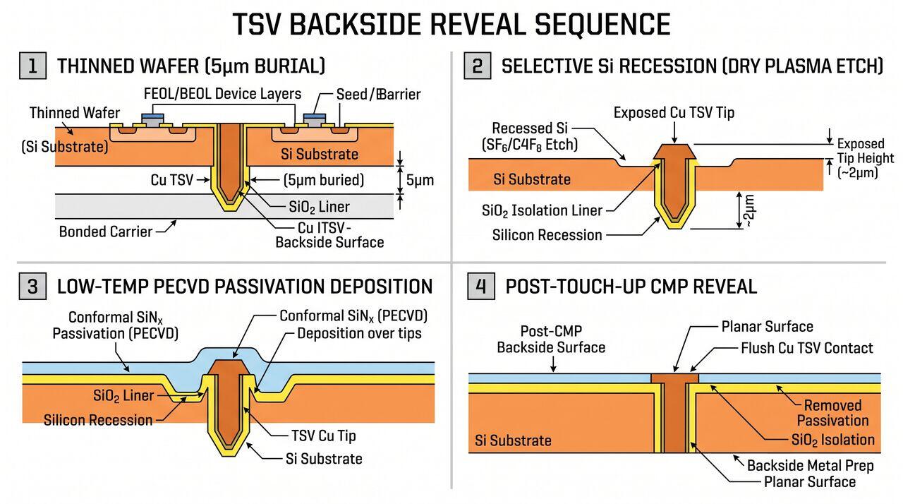
To expose buried copper TSVs from the backside without smearing copper metal across the silicon substrate:
- Coarse/Fine Backgrinding: Stops approximately above the TSV copper tips.
- Silicon Dry/Wet Etching: Selective SF6 plasma or TMAH wet etch selectively recedes the silicon substrate, leaving copper TSV tips protruding above the surface.
- Backside Passivation Deposition: Low-temperature PECVD dielectric deposited over the exposed tips.
- Touch-up CMP Reveal: Chemical mechanical polishing removes dielectric over the TSV tips, leaving perfectly flush, isolated copper contacts ready for micro-bumping or hybrid bonding.
05Summary & Key Takeaways
- DRIE Bosch Process etches smooth, high-aspect-ratio (> 10:1) TSV cavities.
- PPR Electroplating combined with specialized additives achieves void-free TSV copper filling by periodically dissolving top pinch-off overhangs.
- Temporary Wafer Bonding supports thinned wafers down to using laser-debondable thermoplastic adhesives.
- Taiko Backgrinding retains a outer silicon ring to prevent warpage without requiring carrier substrates.
- Controlled TSV Reveal combines selective silicon recessed etching, PECVD passivation, and touch-up CMP.
→Prerequisites & continue reading
Prerequisites: ["p08-t8.2-t1-tsv-wafer-thinning-bspdn-fundamentals.md"]
Also in Topic 8.2, TSVs, Wafer Thinning & Backside Power:
Tier 1 · Through-Silicon Vias (TSV), Wafer Thinning & BSPDN: …Tier 3 · Thermomechanical Stress, TSV Extrusion & Buried Powe…