01High-Level Purpose & Physical Motivation
For over five decades, integrated circuits were designed as strictly two-dimensional (2D) planar structures. Signals and electrical power were routed exclusively through metal layers fabricated on the front side of the silicon wafer. However, as transistor densities scaled into sub-2nm regimes, two major physical barriers emerged:
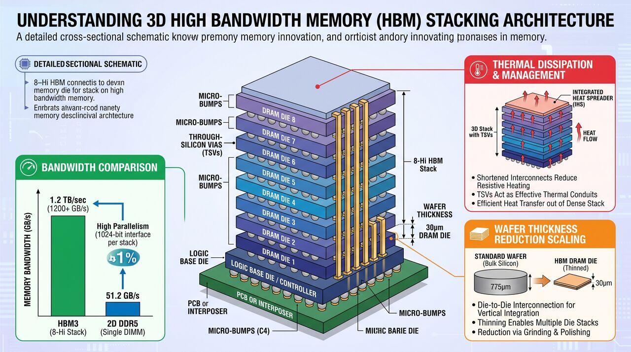
- 2D Interconnect Bottleneck: Connecting high-core-count processors to high-capacity memory (such as High Bandwidth Memory, HBM) across a 2D circuit board introduces severe RC delay, latency, and high parasitic power consumption.
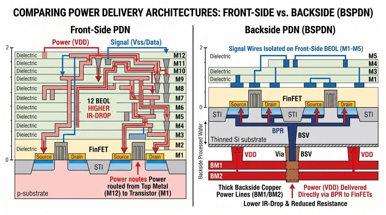
- Front-Side Power Delivery IR-Drop: Sharing front-side BEOL layers between signal wires and power delivery networks creates intense routing congestion. Resistance in thin front-side power lines causes severe voltage drops (IR-drop), limiting maximum compute performance.
To overcome these barriers, semiconductor fabrication has extended into the third dimension (3D) through two revolutionizing technological paradigms:
- Through-Silicon Vias (TSVs) & Wafer Thinning: Vertical electrical connections etched directly through the bulk silicon substrate, enabling high-density vertical stacking of dies (e.g., stacking 8 to 16 DRAM dies in HBM3e/HBM4).
- Backside Power Delivery Networks (BSPDN): Decoupling signal and power networks by moving the entire power distribution grid to the backside of the wafer, connecting directly to transistors through Buried Power Rails (BPR).
02Key Inputs, Outputs & Process Flow
Key Inputs
- Processed Device Wafer: Fully fabricated FEOL/BEOL wafer containing active transistors and front-side interconnect layers.
- Carrier Substrate: Temporary glass or mechanical silicon carrier wafer used to support thinned device wafers.
- Metallization & Insulating Precursors: High-aspect-ratio CVD insulation liners (), PVD barrier/seed (Ti/Cu), and high-speed copper electroplating chemistry.
Key Outputs
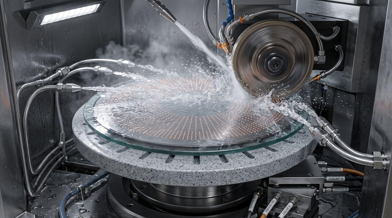
- Ultra-Thin TSV-Enabled Wafer: Silicon substrate thinned from down to , with exposed copper TSVs or backside power contacts ready for 3D stacking or packaging.
03TSV Integration Schemes & Backside Power Delivery Architecture
A. TSV Integration Integration Schemes
Depending on when vertical vias are fabricated during the manufacturing flow, TSVs are classified into three integration schemes:
- Via-First: TSVs etched and filled in bulk silicon before FEOL transistor formation.
- Via-Middle (Industry Standard for 2.5D/3D): TSVs etched and filled after FEOL transistors but before BEOL metallization. Offers optimal balance between thermal budget and via density.
- Via-Last: TSVs etched from the front or backside after BEOL fabrication is complete.
B. Backside Power Delivery Network (BSPDN) Paradigm
In conventional front-side power delivery, electric current (VDD/VSS) must navigate down through 10-15 BEOL metal layers, losing up to of supply voltage to IR-drop.
In BSPDN (e.g., Intel PowerVia, TSMC A16 SPR):
- Signals remain on the front-side BEOL layers.
- Heavy power distribution lines are moved to thick, low-resistance metal layers on the backside of the wafer.
- Power is fed directly up to transistor sources/drains using nano-TSVs or Buried Power Rails (BPR) embedded inside the FEOL shallow trench isolation (STI).
04Conceptual Analogy
Imagine a high-rise office skyscraper:
- Traditional 2D Front-Side Architecture: Trying to fit both the elevator shafts (signals) and massive water supply pipes, electrical mains, and HVAC ducts (power grid) inside the exact same narrow hallway on the front side of every floor. The hallway becomes totally congested, and water pressure drops on upper floors.
- BSPDN & TSV Architecture: Running all heavy electrical mains and plumbing up the back wall of the skyscraper (Backside Power Delivery), while keeping the interior hallways completely clear for fast elevator shafts and pedestrian traffic (Signal BEOL). Building vertical trapdoors through the floors (TSVs) lets you stack multiple skyscraper blocks directly on top of each other.
05Summary & Key Takeaways
- TSVs provide ultra-short vertical electrical connections through the silicon substrate, enabling high-density 3D stacking (e.g., HBM memory).
- Wafer Thinning reduces bulk silicon thickness from to using mechanical backgrinding and CMP.
- Temporary Wafer Bonding is mandatory to mechanically support ultra-thin wafers during backside processing.
- BSPDN (Backside Power Delivery) moves power lines to the rear of the wafer, eliminating IR-drop voltage losses and freeing up front-side routing congestion.
→Prerequisites & continue reading
Prerequisites: ["p08-t8.1-t1-beol-dual-damascene-low-k-fundamentals.md"]
Also in Topic 8.2, TSVs, Wafer Thinning & Backside Power:
Tier 2 · TSV Filling, Taiko Backgrinding & BSPDN Mechanics…Tier 3 · Thermomechanical Stress, TSV Extrusion & Buried Powe…