01Thermomechanical Stress & CTE Mismatch Equations
The integration of large copper Through-Silicon Vias (TSVs) into a monocrystalline silicon substrate introduces severe thermomechanical stress during thermal cycling (e.g., thermal annealing, dielectric deposition, and backend soldering from to ). This stress originates from the massive mismatch in Coefficient of Thermal Expansion (CTE) between copper () and silicon ().
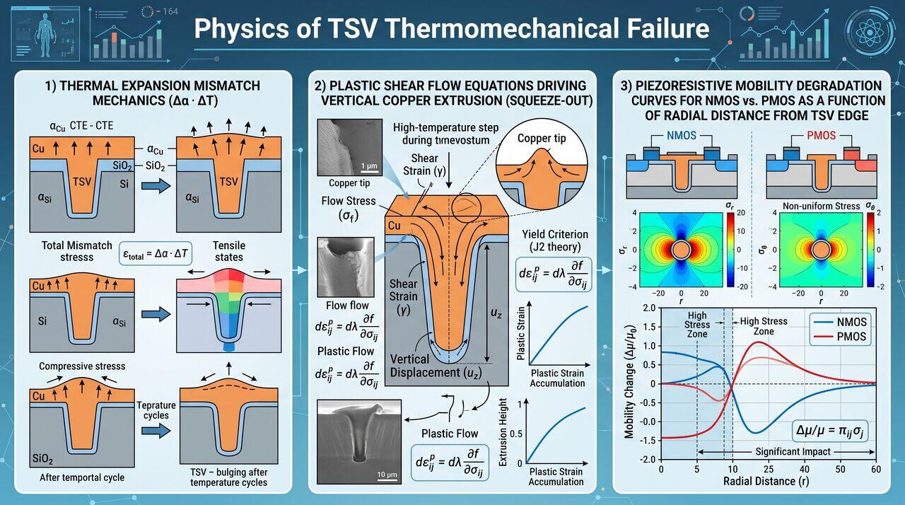
When a TSV cools from an annealing temperature down to room temperature T, the thermal strain mismatch () is:
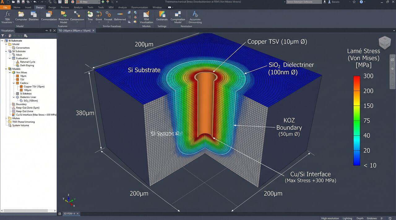
Elastic Stress Field Around Cylindrical TSV (Lame Solution)
Treating the TSV as an elastic cylinder of radius embedded in an infinite silicon matrix, the normal stress components as a function of radial distance r from the via center are given by the Lamé thermal stress equations:
Where:
- : Radial stress (Compressive inside, decaying radially outside)
- : Hoop stress (Tensile along circumferential directions)
- : Young's modulus () and Poisson's ratio (0.28) of silicon
- : Effective temperature change accounting for plastic deformation relaxation
02Piezoresistive Transistor Degradation & Keep-Out Zone (KOZ)
Monocrystalline silicon exhibits strong piezoresistive behavior: mechanical stress alters electron and hole mobility () in transistor channels by distorting energy band structures. The fractional change in carrier mobility () under localized stress tensor components is expressed as:
Where are the piezoresistive coefficients of silicon ().
- PMOS Impact: Compressive axial stress enhances hole mobility, but radial tensile stress degrades performance.
- NMOS Impact: Radial stress causes electron valley splitting, degrading electron mobility by up to .
- Keep-Out Zone (KOZ): To prevent severe drive-current mismatch and timing jitter, electronic design automation (EDA) rules enforce a KOZ boundary (typically to the TSV radius) around every TSV where active transistor placement is strictly prohibited.
03Copper TSV Thermal Extrusion ("Squeeze-Out") Physics
During subsequent high-temperature BEOL processing (), copper expands much faster than silicon. Because the TSV is constrained laterally by the rigid silicon matrix, compressive stress along the vertical axial direction () exceeds the plastic yield strength of electrodeposited copper ().
This drives plastic flow and diffusive creep, causing the copper core to permanently extrude vertically out of the via top, a defect known as TSV Extrusion or "Pop-out":
Extrusion heights of crack overlying thin Low-k dielectric layers, severing BEOL metal interconnect lines.
Remediation Strategy: Wafers undergo a high-temperature Pre-CMP Thermal Stress-Relief Anneal () to force plastic extrusion and grain growth before CMP. Touch-up CMP then grinds away extruded copper, leaving a thermally stable interface.
04Backside Power Delivery (BSPDN) & Buried Power Rails (BPR) Physics
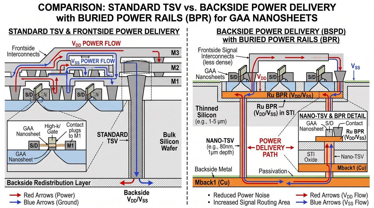
In advanced sub-2nm nodes (e.g., N2/A16), conventional TSVs () are far too large to connect directly to individual transistor cells. BSPDN utilizes nano-TSVs () coupled with Buried Power Rails (BPR):
- Buried Power Rail (BPR) Architecture: Ruthenium (Ru) or Tungsten (W) rails etched inside the shallow trench isolation (STI) oxides between FinFET/GAA nanosheets during MEOL.
- Nano-TSV Direct Contact: Backside grinding exposes the bottom of the BPR rail. Backside metallization connects power directly to BPRs without routing through front-side BEOL layers.
- Electromigration Immunity: Ru power rails exhibit near-zero electromigration at extreme current densities (), eliminating IR-drop by and reducing standard cell area by .
05Summary & Key Takeaways
- CTE Mismatch () generates intense Lamé radial and hoop stress fields around copper TSVs.
- Piezoresistive Stress Effects distort silicon band structure, requiring a Keep-Out Zone (KOZ) exclusion zone for transistor placement.
- Thermomechanical Extrusion causes copper to permanently deform upward during thermal cycles, requiring a pre-CMP stress-relief anneal.
- BSPDN & Buried Power Rails (BPR) utilize sub-100nm nano-TSVs and refractory metals (Ru/W) to eliminate front-side IR-drop and free up signal routing area.
→Prerequisites & continue reading
Prerequisites: ["p08-t8.2-t2-tsv-filling-taiko-backgrinding-bspdn-mechanics.md"]
Also in Topic 8.2, TSVs, Wafer Thinning & Backside Power:
Tier 1 · Through-Silicon Vias (TSV), Wafer Thinning & BSPDN: …Tier 2 · TSV Filling, Taiko Backgrinding & BSPDN Mechanics…