01Introduction: The Nanometer Particle Challenge
As semiconductor features scale below 2nm, a microscopic particle as small as 5 to 10 nm can bridge conductive metal lines or block lithographic light exposure, causing total device failure. Removing nanoscale particles from silicon wafer surfaces requires overcoming massive attractive surface forces.
Particle Removal Efficiency (PRE) is defined as:
Where and are particle counts measured by laser surface inspection tools before and after cleaning.
02What Holds Particles to Wafer Surfaces?
Particles adhere to silicon surfaces through van der Waals attractive forces:
Where is the Hamaker constant (), is particle diameter, and is separation distance (). Because scales linearly with particle diameter , while cleaning removal forces (such as fluid drag) scale with or , smaller particles are exponentially harder to detach.
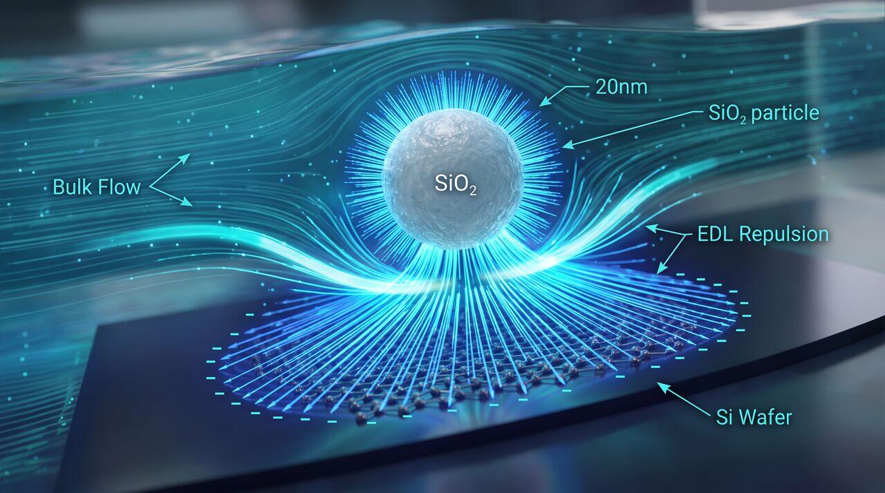
03The Solution: Zeta Potential () & Electrostatic Repulsion
When immersed in aqueous solutions, both the silicon surface and the particle develop an electrical charge layer known as the Electrical Double Layer (EDL). The electrical potential at the slipping plane of this layer is called the Zeta Potential ().
Controlling Zeta Potential with pH
- In Alkaline Solutions (SC-1, pH ~ 10): Both silicon dioxide () surfaces and silicon nitride/slurry particles acquire strongly negative Zeta potentials ( to ). Since like charges repel, a strong electrostatic repulsive force () pushes particles away from the wafer surface, preventing re-deposition!
- In Acidic Solutions (pH < 3): Zeta potentials shift near zero (the Isoelectric Point, IEP), eliminating repulsion and causing rapid particle aggregation and surface contamination.
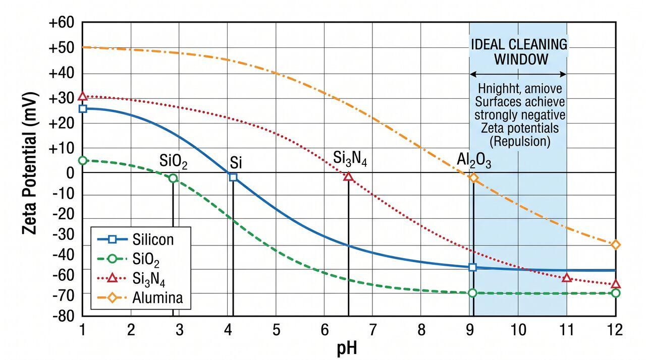
04Key Rules for High PRE in Fabs
- Keep pH High During Cleaning: Always use alkaline chemistries (e.g., dilute SC-1 or ammonia-DIW) when removing particles to maintain strongly negative Zeta potentials ().
- Combine Chemistry with Mechanical Energy: Chemical undercut plus megasonic acoustic streaming provides the detachment force needed to overcome van der Waals attraction.
- Avoid Isoelectric Points (IEP): Never process wafers at liquid pH levels where the wafer or particle Zeta potential crosses zero.
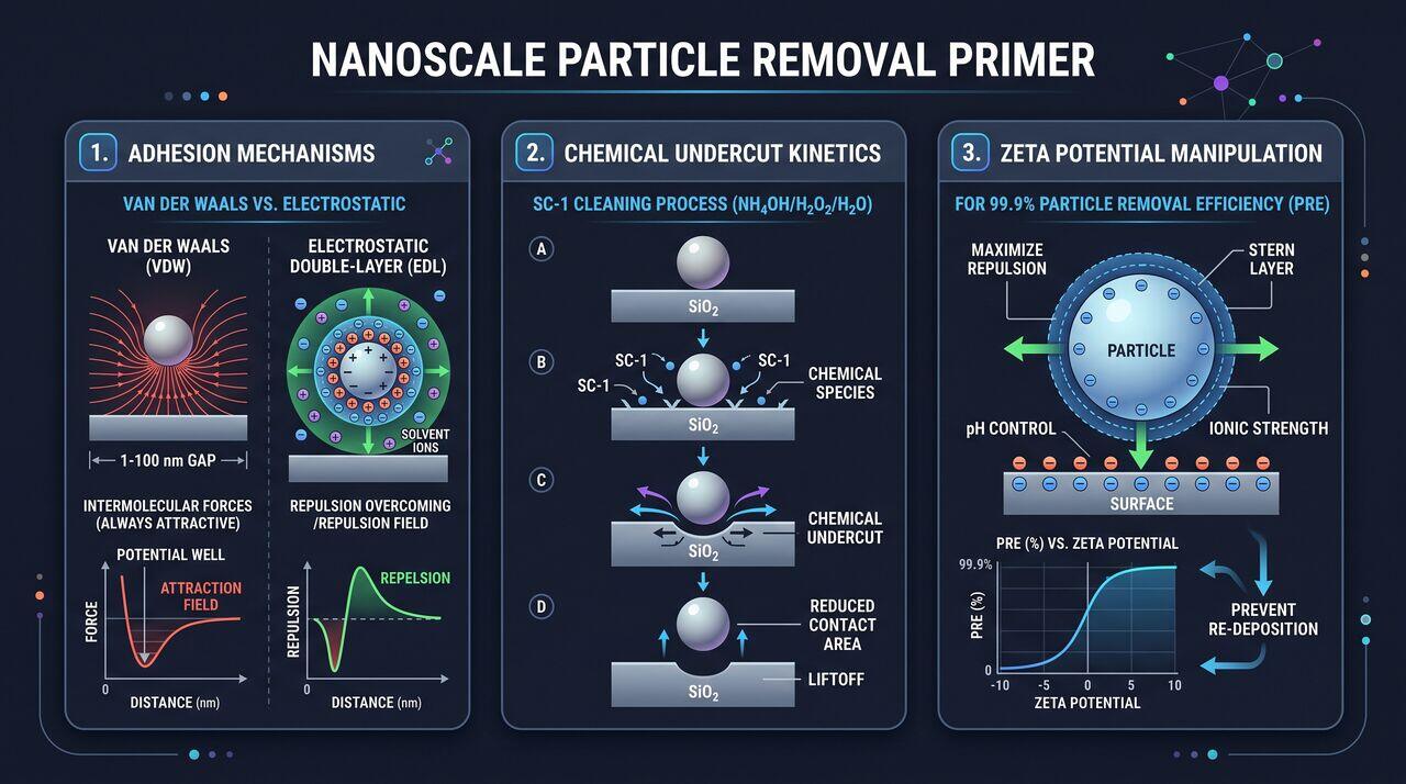
→Prerequisites & continue reading
Prerequisites: General Chemistry, Basic Surface Science
Also in Topic 4.3, Particle Removal & Zeta Potential Engineering:
Tier 2 · Megasonic Transducer Kinematics & Marangoni Drying M…Tier 3 · DLVO Theory, Acoustic Cavitation Dynamics & Supercri…