01Executive Summary
When the semiconductor industry transitioned from aluminum to copper interconnects at the node to eliminate RC signal delay, plasma reactive ion etching of copper proved unfeasible due to the non-volatile nature of copper-halogen compounds. To overcome this hurdle, IBM and industry partners introduced the Damascene process, where dielectric trenches are etched first, filled with electroplated copper, and planarized back using Chemical Mechanical Polishing (CMP). This introductory guide explores the fundamental principles of copper Damascene CMP, the necessity of a two-step polishing sequence, and the role of barrier metal removal.
02Why Copper Requires the Damascene Architecture
Aluminum interconnects were fabricated by subtractive patterning: depositing aluminum across the entire wafer, applying photoresist, and etching away unwanted metal with chlorine plasma (, volatile at low temperatures).
In contrast, copper reaction products (such as ) have extremely low vapor pressures below , making reactive ion etching (RIE) impossible for manufacturing.
The Damascene process reverses this order:
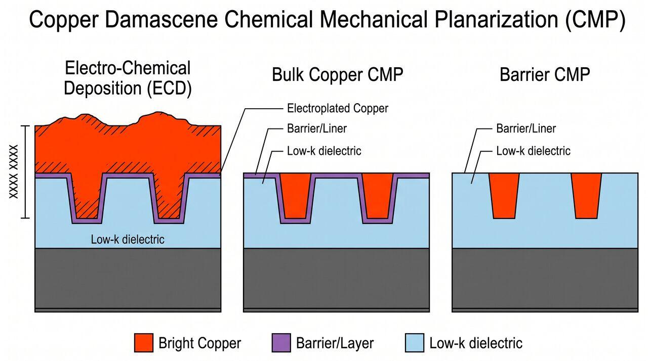
- Etch trenches and via holes into the low-k inter-layer dielectric (ILD).
- Deposit a thin diffusion barrier (e.g., Tantalum/Tantalum Nitride, ) and a copper seed layer via Physical Vapor Deposition (PVD).
- Fill trenches with bulk electroplated copper (Electro-Chemical Deposition, ECD), creating a continuous copper "overburden".
- Perform Copper CMP to remove the overburden, leaving isolated copper wires embedded smoothly in dielectric trenches.
03The Two-Step Polishing Sequence
Polishing a Damascene copper structure requires removing three completely different materials with vastly different mechanical and chemical properties:
- Bulk Copper Overburden (Soft metal, )
- Diffusion Barrier Film () (Extremely hard ceramic metal, )
- Low-k Dielectric Layer (Fragile porous matrix, modulus )
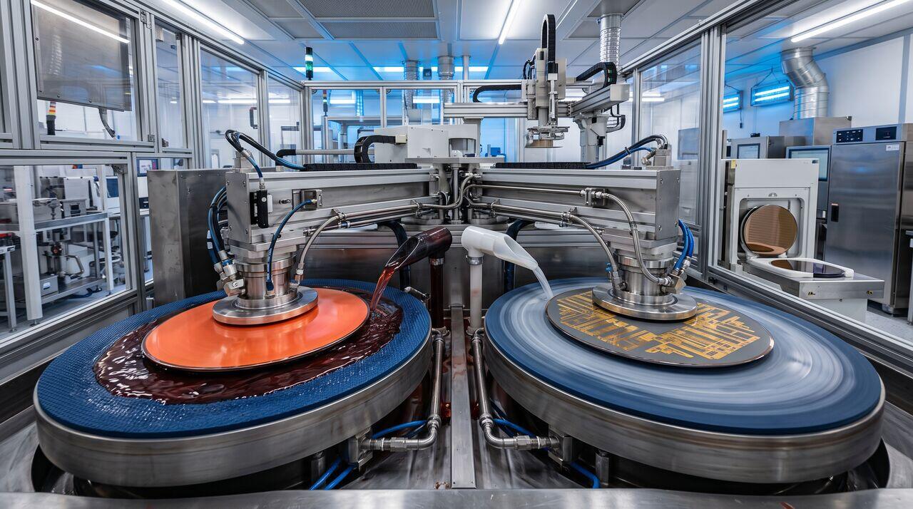
To handle these disparate materials without damaging the fragile low-k dielectric, modern fabs deploy a Two-Step CMP Strategy:
Step 1: Bulk Copper Overburden Removal
- Goal: Rapidly polish away bulk copper down to the barrier layer at rates .
- Chemistry: Acidic or neutral slurry containing hydrogen peroxide () oxidant, organic complexing agents (glycine), and a corrosion inhibitor (Benzotriazole, BTA).
- Selectivity: High selectivity of Copper relative to Tantalum Nitride (). The hard barrier acts as a natural "polish stop" layer.
Step 2: Barrier Metal & Dielectric Planarization
- Goal: Remove the thin barrier layer () across the field while smoothing copper lines and dielectric boundaries.
- Chemistry: Alkaline slurry (pH ) with silica abrasives.
- Selectivity: Tuned to a 1:1:1 selectivity ratio () to ensure all three materials polish at identical rates, preventing step heights.
04Key Challenge: Dishing and Erosion Defects
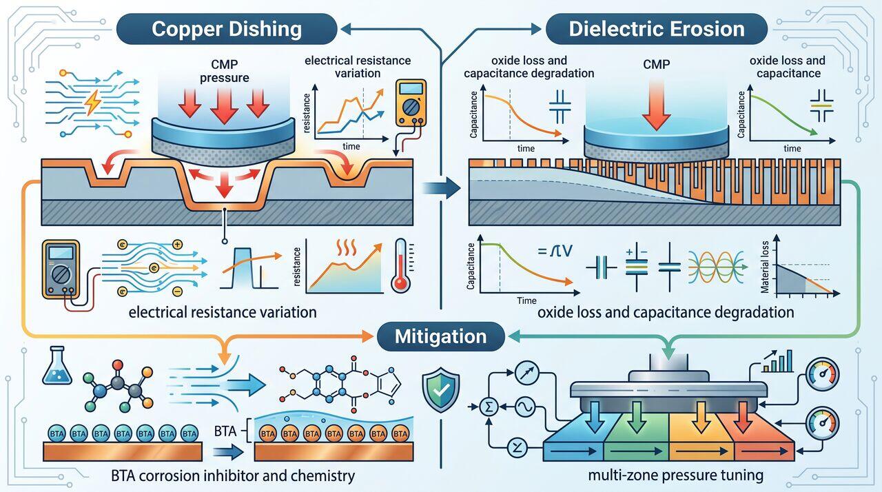
Because copper is significantly softer than the surrounding dielectric, non-uniform polishing can induce topographical defects:
- Copper Dishing: Excessive chemical-mechanical removal of copper within wide wire trenches, causing a concave recession below the dielectric plane.
- Dielectric Erosion: Degradation and thinning of the dielectric oxide in dense array regions containing narrow copper lines, causing localized field sinking.
→Prerequisites & continue reading
Prerequisites: ["p03-t3.1-t1-oxide-polysilicon-cmp-fundamentals"]
Also in Topic 3.2, Copper Damascene & Barrier CMP:
Tier 2 · Barrier Slurry Chemistry & Galvanic Corrosion: Elect…Tier 3 · Dishing & Erosion Tribochemical Models: Sub-10nm Int…