01Executive Summary
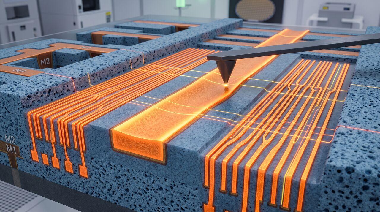
As back-end-of-line (BEOL) interconnect dimensions scale into sub-10nm logic nodes, copper line dishing and dielectric erosion become primary limiters of device yield and signal integrity. Uncontrolled topography variations cause cross-sectional area reductions that spike wire resistance (R), increase inter-line capacitive coupling (C), and induce disastrous electro-migration failures. This advanced monograph presents analytical tribochemical models for dishing and erosion, pad flexure beam dynamics, pattern density dependence, and advanced mitigation strategies.
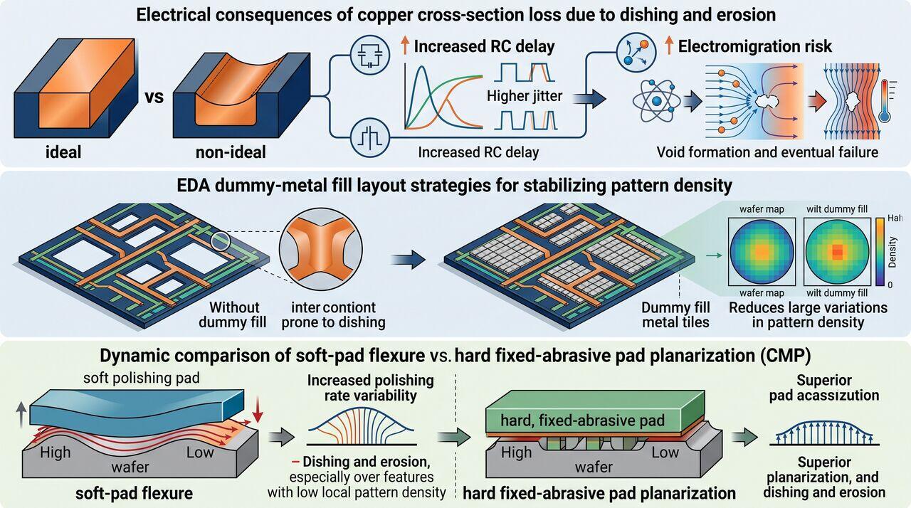
02Topographical Defect Definitions & Electrical Impact
In copper Damascene CMP, the co-polishing of materials with radically different mechanical hardnesses ( vs. ) leads to two distinct topographical defects:
- Copper Dishing (): The vertical recession of the copper surface below the adjacent dielectric boundary in isolated wide lines.
- Dielectric Erosion (): The overall vertical loss of the dielectric oxide matrix within dense arrays of narrow copper lines.
Electrical Resistance & RC Delay Penalty
For a copper wire of nominal width w, height h, and length L, dishing reduces the effective conductor cross-sectional area by . The resulting electrical line resistance R increases non-linearly:
In sub-10nm nodes where wire height , a dishing depth of just causes a spike in line resistance, severely degrading clock frequencies and inducing electromigration voiding.
03Analytical Tribochemical Models for Dishing
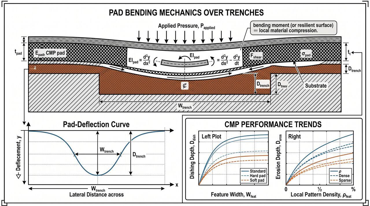
Dishing occurs because the elastic polyurethane polishing pad flexes under applied down-force pressure and dips into soft copper trenches.
2.1 Pad Bending Beam Dynamics
Modeling the polishing pad as an elastic beam with Young's modulus and flexural rigidity , the pad deflection y(x) spanning a copper trench of width w under local pressure is governed by the bi-harmonic bending equation:
Solving boundary conditions at trench edges () yields the maximum central dishing depth :
Where represents the characteristic structural decay length of the pad, and is the elastic foundation modulus.
Key Physical Scaling Laws
- Line Width Dependence (w): Dishing increases exponentially with trench width w. For , dishing is negligible; for wide power rails (), dishing saturates at its maximum limits.
- Over-Polish Time Sensitivity (): Dishing scales linearly with over-polish time:
04Dielectric Erosion Dynamics & Pattern Density Effects
Erosion occurs because dense arrays of copper lines reduce the local areal fraction of hard dielectric, increasing the effective contact pressure on the remaining dielectric features.
Local Pressure Redistribution Model
If a die region has a local copper pattern density (where ), the local effective pressure exerted by the pad onto the dielectric asperities during Step 2 CMP is elevated:
As pattern density , the effective pressure on the remaining dielectric structures spikes dramatically, driving rapid dielectric loss () and localized array sinking.
05Advanced Dishing & Erosion Mitigation Matrix
| Mitigation Strategy | Physical Mechanism | Technical Implementation | Trade-Off |
|---|---|---|---|
| Fixed-Abrasive CMP Pads | Abrasives embedded in rigid resin posts prevent pad flexure into trenches | Ceria/Silica particles bonded to hard composite pad matrix | Higher wafer defectivity & micro-scratching |
| Metal Dummy Fill Insertion | Breaks up wide dielectric fields and wide Cu rails to unify local pattern density | Automated EDA layout dummy metal insertion routines | Increases inter-line parasitic capacitance |
| High-Fixed-Modulus Polyurethane Pads | Elevates pad flexural rigidity , suppressing pad dipping | Hard sub-pads with high elastic modulus () | Degrades wafer-scale macro-uniformity (WIWNU) |
| High-Selectivity Barrier Slurries | Chemical inhibition limits chemical Cu dissolution during Step 2 over-polish | Self-assembled inhibitor monolayers (BTA/Triazoles) | Tightens process window for complete barrier removal |
→Prerequisites & continue reading
Prerequisites: ["p03-t3.2-t2-barrier-slurry-chemistry-galvanic-corrosion"]
Also in Topic 3.2, Copper Damascene & Barrier CMP:
Tier 1 · Copper Damascene & Barrier CMP Fundamentals: Multi-S…Tier 2 · Barrier Slurry Chemistry & Galvanic Corrosion: Elect…