01Executive Summary
As semiconductor manufacturing scaled into sub-micron and nanometric regimes, traditional etch-back and reflow techniques became incapable of maintaining the ultra-flat topography required for high-resolution photolithography. Chemical Mechanical Polishing (CMP) emerged as the indispensable unit operation that combines chemical reactivity and mechanical abrasion to achieve global wafer planarization. This fundamental guide explores the core principles of oxide and polysilicon CMP, the synergistic interaction between chemical slurries and polyurethane pads, and why CMP is essential for modern multi-level integrated circuits.
02The Critical Need for Global Planarization
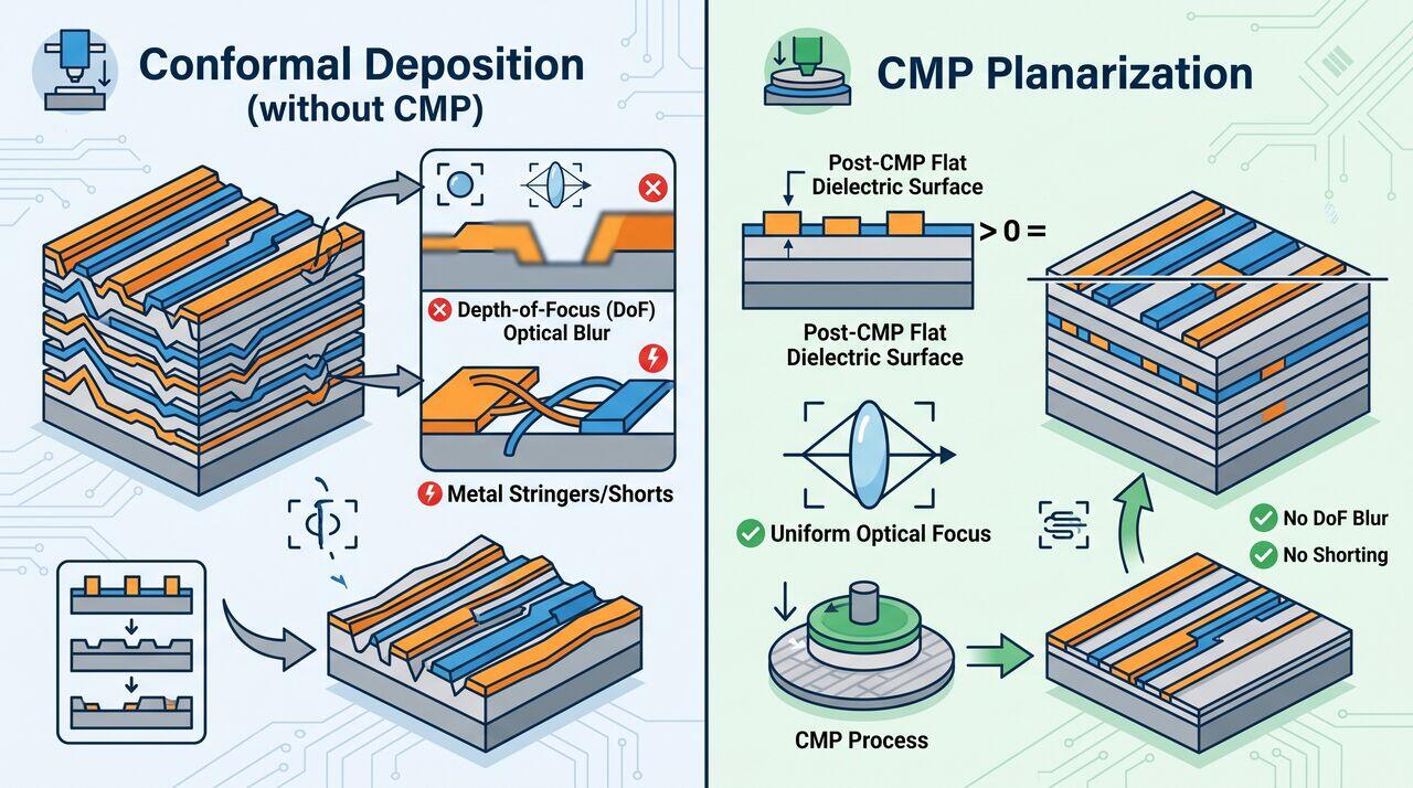
In early integrated circuit fabrication, depositing dielectric layers (such as silicon dioxide, ) over patterned metal lines or polysilicon gates resulted in a conformal, undulating surface topography. As multiple interconnect layers were stacked vertically, these topography variations accumulated, leading to severe operational bottlenecks:
- Photolithographic Depth-of-Focus (DOF) Loss: High-numerical-aperture (NA) stepper lenses have an extremely narrow depth of focus (often ). Non-planar surfaces cause feature defocusing and critical dimension (CD) variations.
- Metal Interconnect Stringers: Sub-surface steps cause metal pooling during BEOL deposition, leading to electrical shorts between adjacent interconnect lines.
- Mechanical Stress & Crack Propagation: Non-uniform film thicknesses introduce localized stress concentrations that induce dielectric cracking during thermal cycling.
03Fundamental Mechanics: Synergism of Chemistry and Mechanics
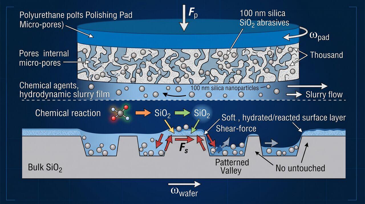
CMP operates through a dual material-removal mechanism where chemistry and mechanical wear act synergistically. Neither mechanism alone achieves high removal rates with low surface damage:
- Chemical Action: The slurry contains reactive chemicals (such as potassium hydroxide, , or ammonium hydroxide, , for silica polishing) that hydrate and soften the outer atomic layers of the wafer surface, creating a pliable hydrated silica film:
- Mechanical Action: Sub-micron abrasive nanoparticles (typically colloidal silica or ceria, ) suspended in the slurry are pressed into the hydrated surface film by a rotating polyurethane pad. The shear force generated by pad motion micro-scratches and shears away the softened hydrated material.
04Preston's Law of Material Removal
The foundational empirical relationship governing material removal in CMP is Preston's Law (1927):
Where:
- is the Material Removal Rate (nm/min or Å/min).
- is Preston's Coefficient (Pa), capturing chemical reactivity, temperature, pad roughness, and abrasive morphology.
- P is the applied down-force pressure (kPa or psi).
- V is the relative linear velocity between the wafer surface and the polishing pad (m/s).
Key Takeaway for Operators
To increase polishing throughput, one can either increase down-force pressure or increase platen rotation speed. However, excessive pressure increases defectivity (micro-scratches), while excessive velocity reduces slurry residence time and increases frictional heating.
05Key Process Components: Tool, Pad, and Slurry
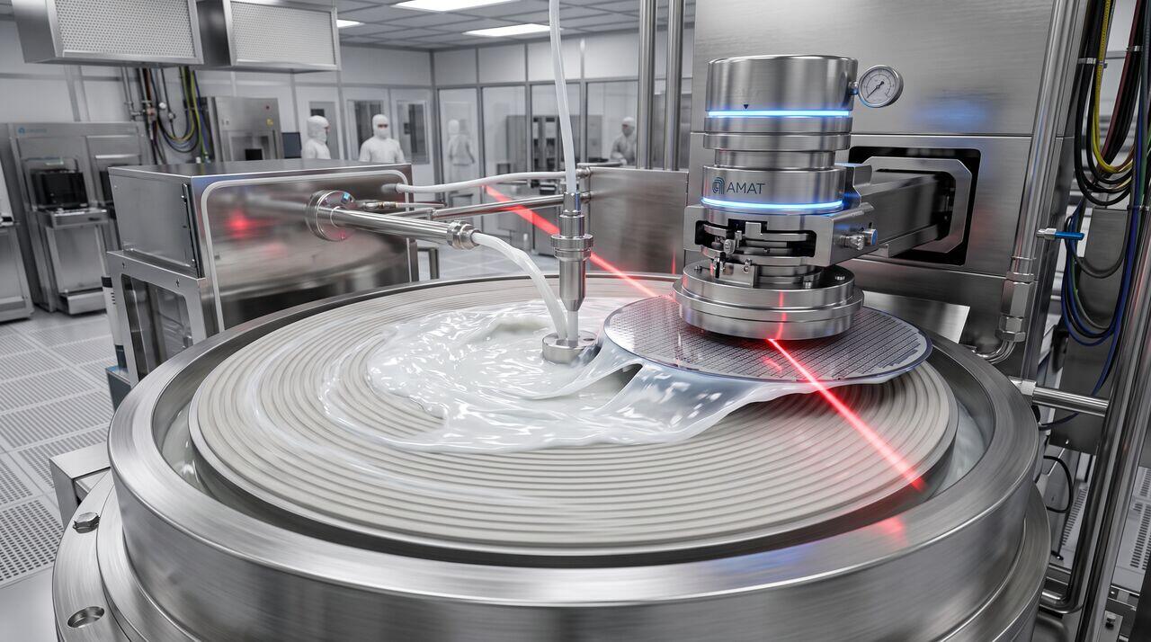
A standard CMP system consists of four primary subsystems:
| Subsystem | Primary Function | Key Material Specifications |
|---|---|---|
| Platen & Pad | Provides mechanical backing and slurry transport channels | Rigid polyurethane foam with closed-cell pore structures |
| Carrier Head | Retains wafer, applies controlled multi-zone down-force | Pneumatic retaining rings and multi-zone flexible membranes |
| Slurry Dispenser | Delivers controlled flow of chemical-abrasive suspension | pH 10–11 (Oxide/Silica) or pH 2–3 (Ceria), abrasive particles |
| Diamond Conditioner | Sweeps pad surface to restore micro-roughness and open pores | Electroplated diamond grit disk operating under in-situ rotation |
→Prerequisites & continue reading
Prerequisites: ["p02-t2.3-t1-edge-profiling-lapping-etching-fundamentals"]
Also in Topic 3.1, Oxide & Polysilicon CMP:
Tier 2 · Prestonian Kinematics & CMP Tool Architecture: Press…Tier 3 · Tribology & Luo-Dornfeld Abrasive Mechanics: Micro-S…