01Executive Summary & Solid-State Chemical Physics
The transition from a mechanically lapped wafer to an atomically pristine silicon substrate represents a shift from mechanically driven indentation fracture to chemically governed reaction kinetics.
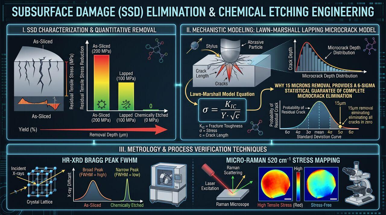
While double-side lapping relies on three-body abrasive contact mechanics to achieve global geometric parallelism (), it inevitably leaves a thin, uniform layer of subsurface damage (SSD), consisting of micro-cleavage cracks, dislocation tangles, and residual surface tensile stress ().
Chemical stress-relief etching must completely dissolve this damaged crystalline region while maintaining strict control over surface micro-waviness () and Within-Wafer Non-Uniformity (). Achieving this requires precise engineering of liquid-solid boundary layer hydrodynamics and chemical dissolution kinetics.
02Tribochemistry & Indentation Fracture Mechanics in Lapping
During planetary double-side lapping, material removal operates in a hybrid mechanic-tribochemical regime.
Lapping SSD Depth Prediction Formula
Applying Lawn and Marshall's sharp indenter fracture model to rolling abrasive grains under plate pressure P gives the depth of lapping-induced median microcracks ():
Where:
- = Empirical tribochemical coupling factor ().
- = Mean diameter of lapping abrasive grains ( for alumina).
- P = Applied downward plate pressure ().
- = Silicon hardness ().
- = Mode-I Fracture toughness ().
Quantitative Engineering Rule:
To guarantee complete elimination of all slicing and lapping microcracks, the minimum required chemical etch removal depth () must strictly satisfy:
In commercial manufacturing, setting total ( per side) provides a statistical guarantee of total SSD elimination.
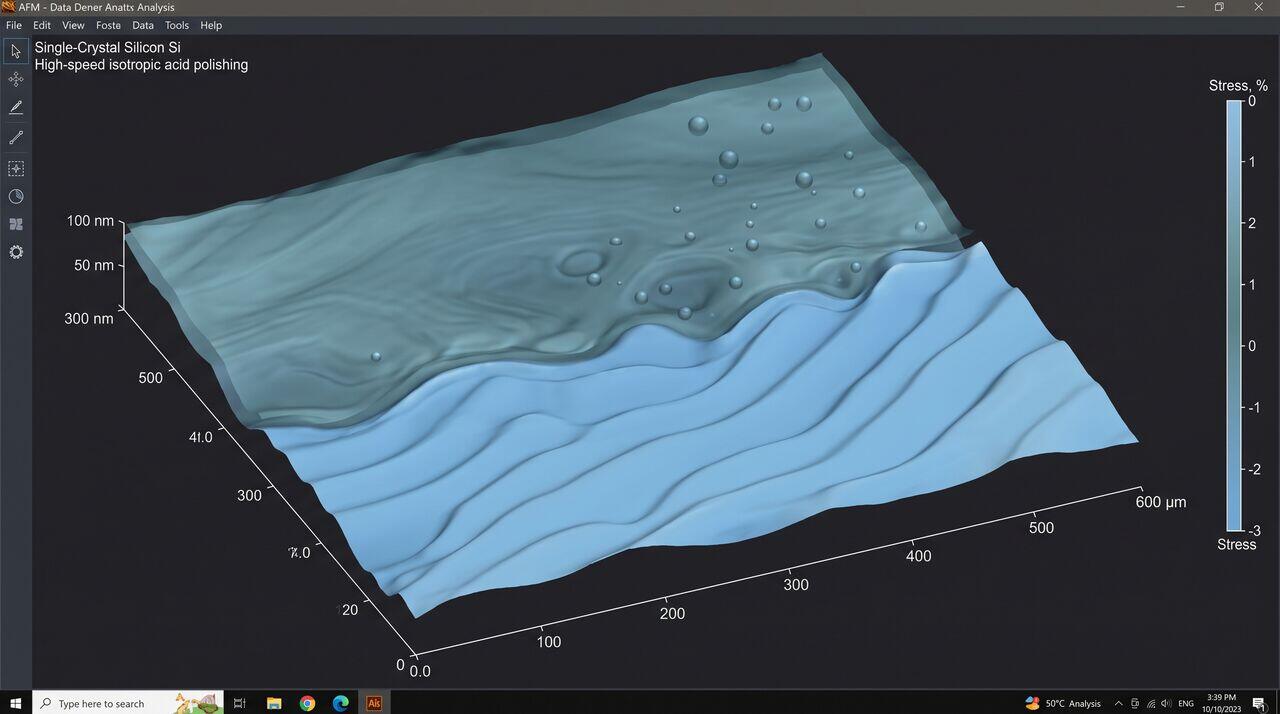
03Chemical Kinetics & Thermodynamics of Acidic Polishing ()
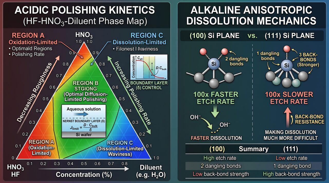
Acidic silicon etching utilizing Nitric Acid (), Hydrofluoric Acid (), and Diluent (Water or Acetic Acid ) is governed by ternary phase diagram kinetics.
The Three Kinetic Regimes
- Region A (High , Low - Oxidation Limited): The dissolution rate of by exceeds the rate of silicon oxidation by . Etching is controlled by chemical oxidation kinetics, producing anisotropic surface pitting along dislocation sites.
- Region B (Balanced High & High - Optimal Polishing): Etching rate reaches a maximum (). The reaction is controlled by viscous liquid diffusion of reactants through the hydrodynamic boundary layer, producing smooth, isotropic polishing.
- Region C (Low , High - Dissolution Limited): Oxidation is extremely fast, forming a continuous passivation layer of . Etching is limited by mass transport, generating long-period surface waviness ().
Mathematical Boundary Layer Mass Transport Model
The dissolution flux () in the optimal diffusion-limited polishing regime is governed by Fick's First Law across Nernst hydrodynamic boundary layer thickness :
Where boundary layer thickness depends on bath fluid agitation velocity U and fluid viscosity :
Process Design Consequence: Sub-millimeter flow velocity variations (U) across the wafer face cause local boundary layer thickness variations (), leading to Within-Wafer Non-Uniformity (WIWNU). Modern wet etch tanks utilize vertical laminar flow spargers and high-frequency bath oscillation () to enforce uniform across the entire substrate.
04Quantum Mechanics of Anisotropic Alkaline Dissolution ()
Alkaline dissolution in potassium hydroxide () or tetramethylammonium hydroxide () exhibits extreme crystallographic anisotropy, where Etch Rate .
Quantum Chemical Mechanism
- Hydroxide Insertion: Hydroxide ions () attack surface silicon atoms, replacing hydrogen-terminated bonds.
- Back-Bond Polarization: The high electronegativity of oxygen polarizes underlying back-bonds, making them susceptible to nucleophilic attack by water molecules ().
- Cleavage Anisotropy: On surfaces, each atom has 2 back-bonds holding it to the crystal lattice, making removal energetic barrier low (). On surfaces, each atom is anchored by 3 strong back-bonds, creating a high activation energy barrier () that slows dissolution by a factor of !
05Metrology & Residual Stress Characterization
To verify total stress relief and defect elimination, finished substrates undergo two rigorous analytical characterization methods:
Residual Lattice Stress Elimination Profile
→Prerequisites & continue reading
Prerequisites: Lapping & Etching Kinematics (Tier 2), Quantum Chemistry, Advanced Fluid Mechanics
Also in Topic 2.3, Edge Profiling, Lapping & Stress-Relief Etching:
Tier 1 · Wafer Edge Profiling, Lapping, and Stress-Relief Etc…Tier 2 · Lapping & Etching Kinematics: Planetary Carrier Dyna…