01The High-k Concept & Equivalent Oxide Thickness (EOT)
The capacitance (C) of a planar gate capacitor is given by:
Where:
- (or k) is the relative dielectric constant ().
- is the vacuum permittivity ().
- A is the gate area.
- is the physical thickness of the dielectric.
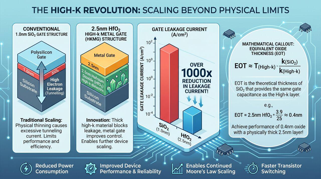
By replacing with a High-k dielectric like Hafnium Oxide (, ), process engineers can increase the physical film thickness by a factor of 5 to 6 while maintaining the exact same capacitive gate drive control!
The metric used to compare high-k films against is Equivalent Oxide Thickness (EOT):
A thick layer () yields an EOT of only , providing massive gate drive current while suppressing quantum tunneling leakage by several orders of magnitude.
02Why Metal Gates Replaced Polysilicon
When high-k dielectrics were initially placed under traditional polysilicon gate electrodes, two major failure modes occurred:
- Polysilicon Depletion: A charge-depleted layer formed at the poly-Si/dielectric interface, adding of unwanted parasitic EOT.
- Fermi-Level Pinning: Chemical reactions between poly-Si and pinned the threshold voltage (), making transistors difficult to turn off.
Replacing polysilicon with Metal Gates (such as Titanium Nitride or Tantalum Nitride ) eliminated polysilicon depletion completely and enabled precise work function engineering for NMOS and PMOS devices.
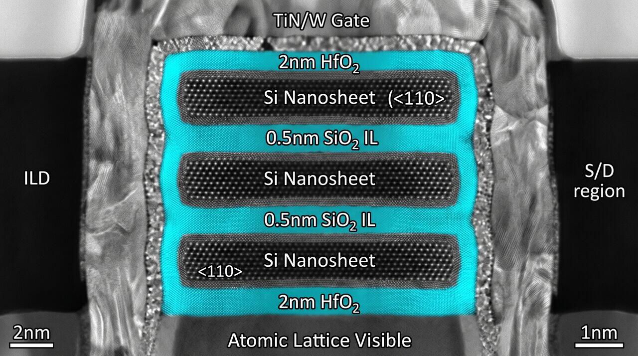
03Principles of Atomic Layer Deposition (ALD)
Because high-k films must be deposited uniformly inside deep 3D FinFET and GAA nanosheet structures with sub-nanometer thickness control, physical vapor deposition (PVD) and chemical vapor deposition (CVD) are inadequate.
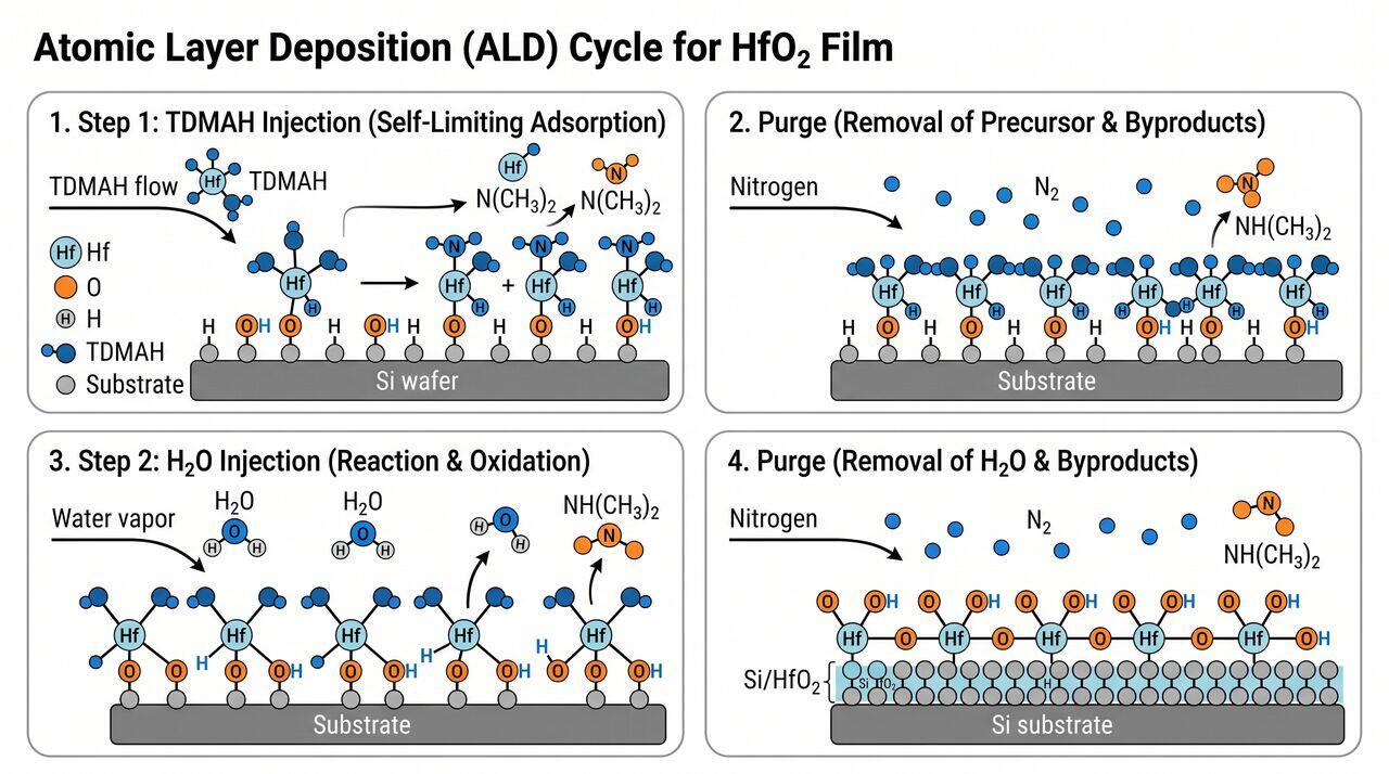
Atomic Layer Deposition (ALD) is a specialized form of CVD based on self-limiting sequential surface reactions:
Each 4-step ALD cycle deposits precisely one atomic monolayer (~), achieving 100% conformal step coverage across complex 3D topographies.
→Prerequisites & continue reading
Prerequisites: ["p07-t7.1-t1-thermal-oxidation-deal-grove-fundamentals"]
Also in Topic 7.2, ALD & High-k Metal Gate Stacks:
Tier 2 · ALD Reactor Hardware: Precursor Pulsing, Purging & C…Tier 3 · Interface Engineering, Dipole Formation & Work Funct…