01Interfacial Layer (IL) Engineering & Chemical Scavenging
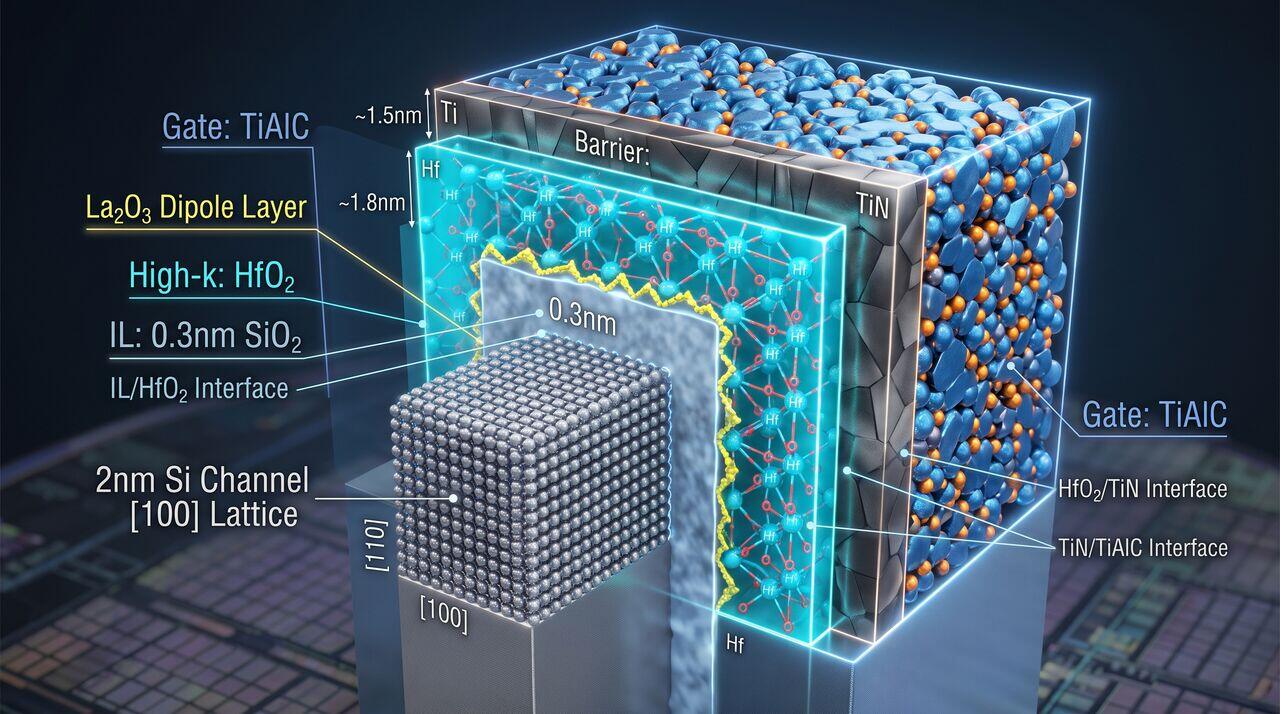
To suppress interface states , a ultra-thin, high-quality Interfacial Layer (IL) of or SiON (~) must be formed prior to ALD.
However, this lower-k layer acts in series capacitance with the film, capping the minimum achievable EOT:
To scale EOT below in sub-2nm nodes, process engineers use Chemical Scavenging:
- Oxygen-scavenging metals (such as Ti, Al, or Hf metal cap layers) are deposited above the high-k stack.
- During high-temperature annealing (), the scavenging metal pulls oxygen atoms out of the underlying interfacial layer through the film, thinning the IL down to without increasing .
02Work Function Metal Tuning for NMOS and PMOS
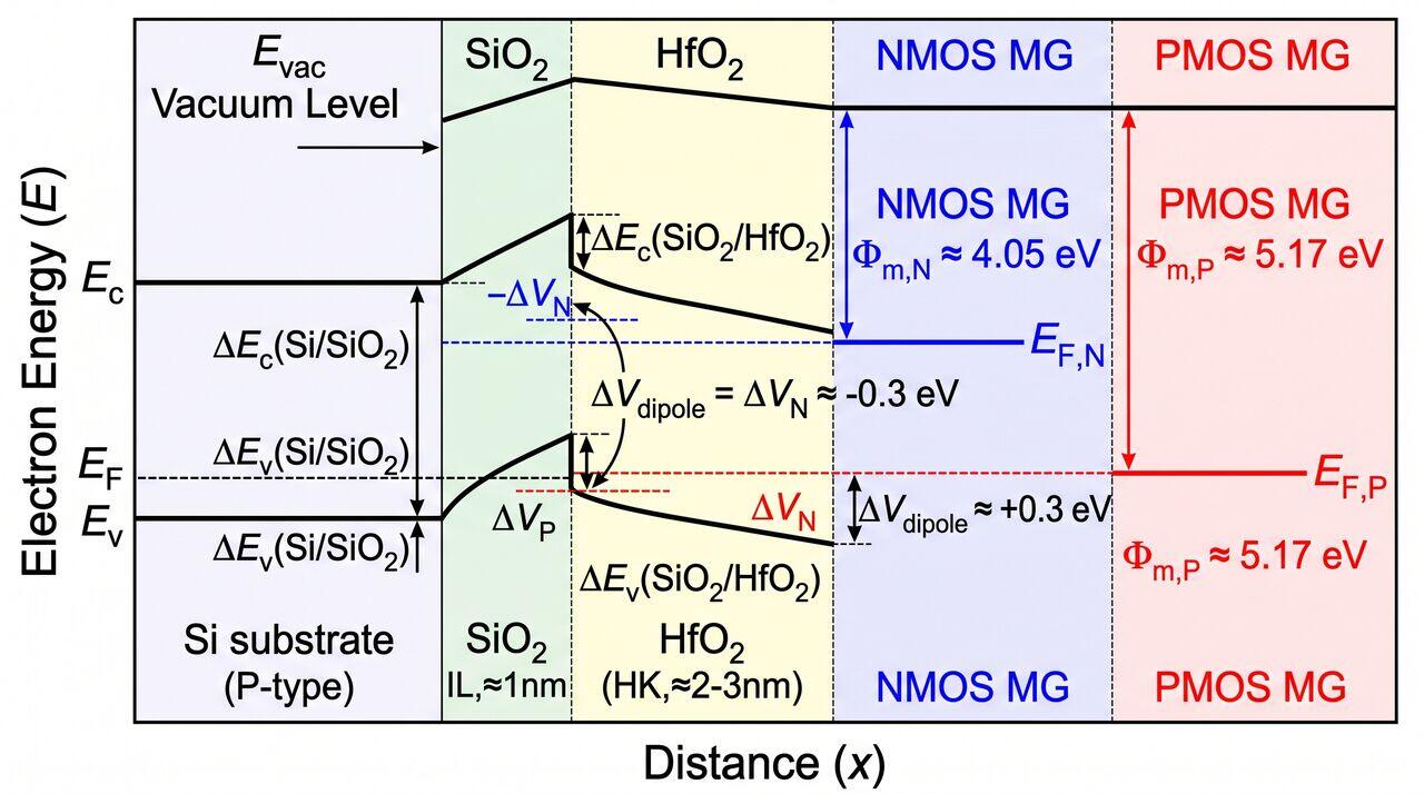
To achieve target threshold voltages () without heavy channel doping (which causes random dopant fluctuation), the effective work function () of the metal gate electrode must match the conduction and valence band edges of silicon:
- NMOS Target Work Function (Band-Edge): (near Si conduction band ).
- PMOS Target Work Function (Band-Edge): (near Si valence band ).
Metal Stack Formulations:
- NMOS Metal Gates: Aluminum-doped titanium carbide () or titanium aluminum nitride (). Aluminum diffusion lowers the metal work function toward .
- PMOS Metal Gates: Stoichiometric titanium nitride () or molybdenum nitride () with high nitrogen content, achieving work functions above .
03Interface Dipole Engineering ( vs. )
An alternative or complementary technique to work function metal switching is Interface Dipole Engineering:
- NMOS Dipole Cap ( / ): Deposition of a sub-monolayer () of Lanthanum Oxide at the interface creates a net interfacial dipole vector pointing toward the silicon substrate, shifting the threshold voltage negatively by up to .
- PMOS Dipole Cap (): Deposition of Aluminum Oxide creates a dipole vector pointing in the opposite direction, shifting positively by .
→Prerequisites & continue reading
Prerequisites: ["p07-t7.2-t2-ald-reactor-hardware-precursor-pulsing-kinematics"]
Also in Topic 7.2, ALD & High-k Metal Gate Stacks:
Tier 1 · Atomic Layer Deposition (ALD) & High-k Metal Gate (H…Tier 2 · ALD Reactor Hardware: Precursor Pulsing, Purging & C…