01Advanced Physical Principles & Mask 3D (M3D) Waveguide Phenomena
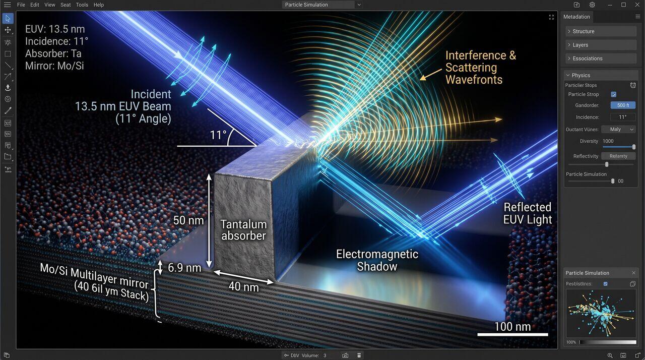
Unlike transmissive photomasks used in DUV lithography where absorbers are ultra-thin chrome films, an EUV photomask is a complex 3D reflective structure. It consists of a thick absorber stack (typically 50-70 nm of Tantalum-based alloys or Low-n phase shift materials) sitting on top of a 40-pair Mo/Si multilayer mirror.
At 13.5 nm wavelength, the physical height of the absorber stack (50 nm) is nearly 4 times larger than the light wavelength. When oblique incident EUV light hits these deep mask absorber trenches, three severe Mask 3D (M3D) electromagnetic effects occur:
- Mask Shadowing Effect: The absorber stack casts a physical shadow over the reflective Mo/Si surface, causing printed feature widths to vary depending on line orientation (Horizontal vs. Vertical) and pitch.
- Phase-Induced Focus Shift: Scattering off absorber sidewalls creates a phase mismatch between diffracted orders, shifting the best focus position as a function of feature size.
- Telecentricity Degradation: Oblique reflection breaks the optical symmetry of diffracted orders entering the projection pupil, causing pattern placement errors during focus variations.
02Anamorphic Transformation Matrix & Kinematics
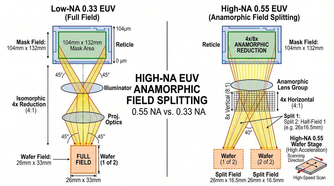
To eliminate M3D shadowing at 0.55 High-NA while maintaining a standard \(26\text{ mm} \times 33\text{ mm}\) reticle size, High-NA EUV projection systems implement an Anamorphic Optical Mapping:
Because the Y-axis reduction is doubled (8x reduction), the exposure field size on the wafer per scan is halved along the Y-axis (from 33 mm down to 16.5 mm), creating a "half-field" exposure footprint.
03EUV Flare Physics & Carbon Nanotube (CNT) Pellicle Dynamics
3.1 Atomic Roughness and Scattered EUV Flare
Because EUV light wavelengths are extraordinarily short (13.5 nm), even sub-nanometer atomic surface roughness (\(\sigma_{\text{rms}} \sim 0.1\text{ nm}\)) on Mo/Si mirrors causes Rayleigh scattering, generating diffuse background illumination known as EUV Flare:
Scattered flare light reduces the optical contrast (Normalized Image Log-Slope, NILS) across the entire exposure field, requiring computational Flare Compensation (FC) during mask data preparation.
3.2 High-Power CNT Pellicle Mechanics
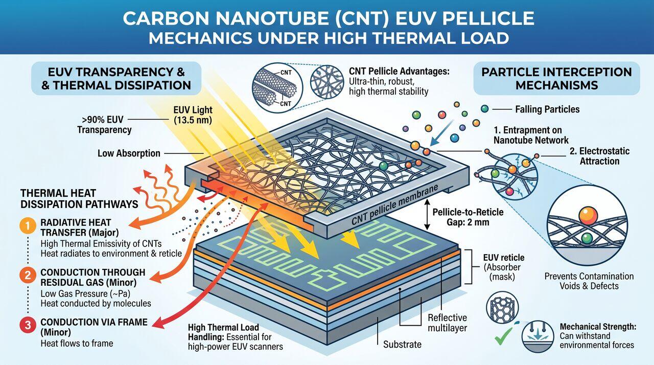
At 0.55 High-NA, EUV power levels reaching the mask exceed 600 Watts/cm². Traditional silicon-based pellicles (thin protective membranes suspended above the reticle) warp and melt under this thermal load. High-NA EUV employs Carbon Nanotube (CNT) pellicles:
- Thermal Endurance: CNT membranes withstand thermal dissipation up to \(1000^\circ\text{C}\) in high vacuum.
- EUV Transmission: Achieves \(> 90\%\) single-pass EUV transparency while capturing sub-micron airborne particles.
04Media Companion Prompts
Media Prompt 1 (Photorealistic Render)
- Prompt: A high-end scientific visualization showing an extreme close-up of an EUV photomask 3D absorber structure. An incident 13.5 nm soft X-ray light beam strikes the tantalum absorber wall at an 11-degree angle, casting a defined electromagnetic shadow onto the underlying Mo/Si multilayer mirror. Interference wave fronts scatter off the absorber edge, rendered in glowing cyan and gold vector physics lines.
Media Prompt 2 (Technical Vector Diagram)
- Prompt: A technical optic vector diagram illustrating High-NA EUV Anamorphic field splitting. Shows a comparison between a full 26x33 mm 0.33 NA exposure field and a halved 26x16.5 mm High-NA 0.55 exposure field. Displays the 4x horizontal / 8x vertical reduction ray matrix entering the anamorphic lens group down to the high-acceleration wafer stage.
Media Prompt 3 (Educational Infographic)
- Prompt: An educational infographic detailing Carbon Nanotube (CNT) EUV Pellicle mechanics under high thermal load. Shows a cross-section of a CNT pellicle membrane suspended 2 mm above an EUV reticle. Highlights thermal heat dissipation pathways (radiation vs. conduction), EUV transparency ray passage (>90%), and particle interception mechanisms preventing reticle contamination voids.
→Prerequisites & continue reading
Prerequisites: ["p05-t5.2-t2-euv-tin-plasma-source-anamorphic-mirrors-mechanics"]
Also in Topic 5.2, EUV & High-NA EUV Lithography:
Tier 1 · Extreme Ultraviolet (EUV) Lithography: Fundamentals …Tier 2 · EUV Tin Plasma Source & Anamorphic Mirror System Mec…