01Introduction & Paradigm Shift
When semiconductor feature sizes scaled below the 10 nm technology node, 193i DUV immersion lithography reached its economic and physical limits. Continuing to scale with DUV required complex multi-patterning techniques (such as SAQP, Self-Aligned Quadruple Patterning) involving up to 4 to 6 separate mask exposures for a single layer, ballooning manufacturing cost and defectivity.
Extreme Ultraviolet (EUV) lithography solved this complexity by making a radical leap in light wavelength: dropping from 193.3 nm down to 13.5 nm, a soft X-ray regime. Because 13.5 nm EUV light is strongly absorbed by virtually all matter (including air, nitrogen, and traditional optical glass lenses), EUV scanners operate entirely inside a high-vacuum chamber and utilize reflective optics (mirrors) instead of refractive lenses.
02Key Process Inputs & Outputs
- Inputs:
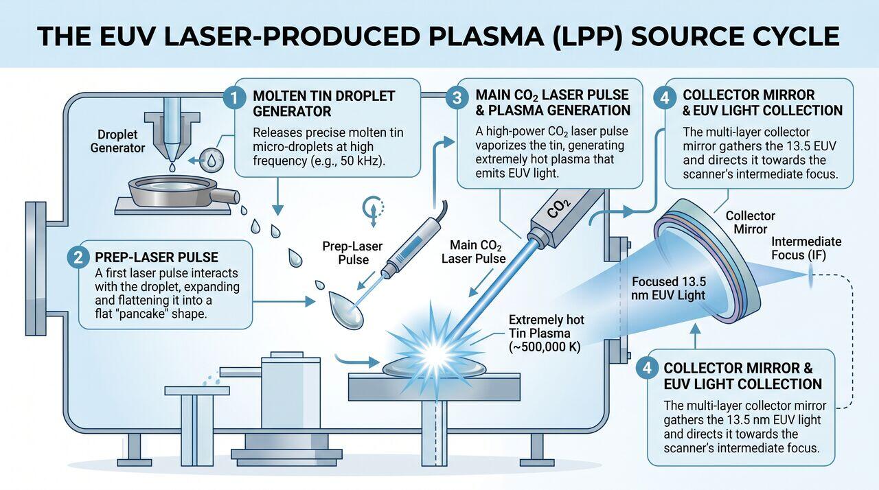
- Light Source: Laser-Produced Plasma (LPP) generated by firing high-power \(\text{CO}_2\) lasers at microscopic molten tin (Sn) droplets 50,000 times per second.
- Optical System: Extreme high-vacuum chamber containing molybdenum/silicon (Mo/Si) multi-layer Bragg reflective mirrors with atomic-scale flatness.
- EUV Mask: Ultra-low expansion glass (ULE) coated with 40-50 pairs of Mo/Si layers and a patterned tantalum-based absorber layer.
- Outputs:
- Ultra-Fine Pattern Resolution: Single-exposure pattern printing down to 26 nm pitch with 0.33 NA EUV, and down to 16 nm pitch with 0.55 High-NA EUV.
03The Generational Shift: Standard 0.33 NA vs. High-NA 0.55 EUV
To extend EUV beyond the 2 nm node without returning to costly multi-patterning, ASML developed High-NA EUV (the EXE scanner platform):
| Scanner Metric | Standard EUV (NXE Series) | High-NA EUV (EXE Series) |
|---|---|---|
| Wavelength (\(\lambda\)) | 13.5 nm | 13.5 nm |
| Numerical Aperture (NA) | 0.33 NA | 0.55 NA |
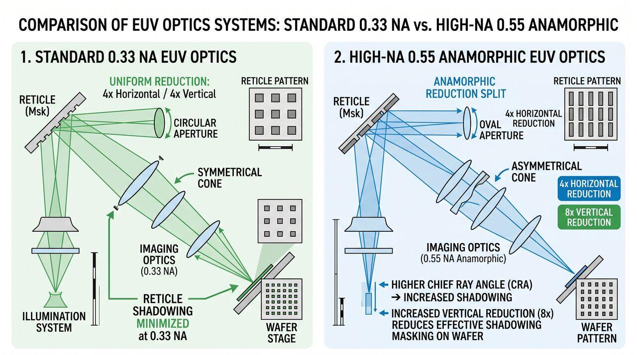
| Lens/Mirror Architecture | Isomorphic (4x reduction X & Y) | Anamorphic (4x reduction X, 8x reduction Y) |
| Single-Exposure Half-Pitch | \(\sim 13\text{ nm}\) | \(\mathbf{< 8\text{ nm}}\) |
| Wafer Stage Speed / Accel | \(4\text{ m/s}^2\) | \(\mathbf{10\text{ m/s}^2}\) (Ultra-High Speed) |
04Media Companion Prompts
Media Prompt 1 (Photorealistic Render)
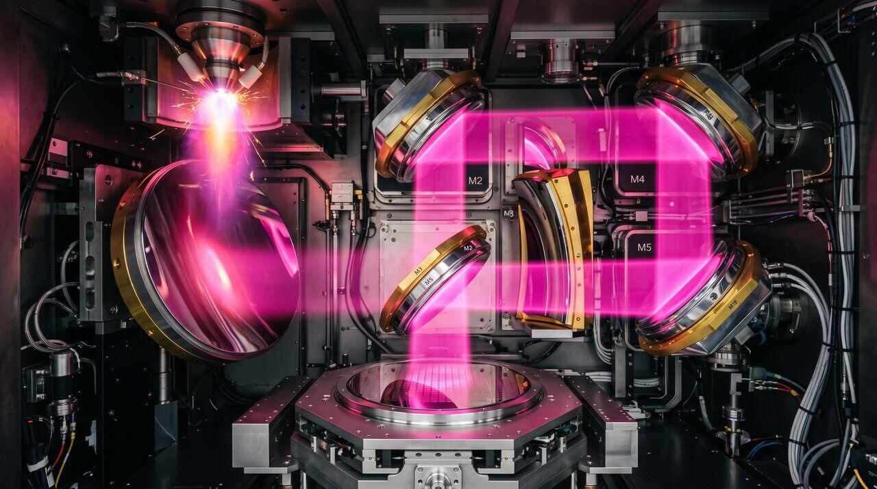
- Prompt: A striking, cinematic photorealistic view inside an ASML High-NA EUV scanner high-vacuum chamber. A glowing magenta-pink laser-produced tin plasma droplet sparks at the source. The intense 13.5 nm light reflects off a series of massive, mirror-polished curved Mo/Si Bragg mirrors, directing a precise rectangular light beam onto a silicon wafer stage. Ultra-clean aerospace vacuum chamber design, gold and chrome optical mounts, futuristic technology, 8k resolution.
Media Prompt 2 (Technical Vector Diagram)
- Prompt: A technical comparison diagram illustrating Standard 0.33 NA EUV optics vs. High-NA 0.55 Anamorphic EUV optics. Shows light ray cones reflecting from the reticle to wafer stage. Highlights the 4x/4x uniform reduction in 0.33 NA versus the anamorphic 4x horizontal / 8x vertical reduction split in High-NA 0.55 optics to prevent reticle shadow masking.
Media Prompt 3 (Educational Infographic)
- Prompt: An educational infographic explaining the EUV Laser-Produced Plasma (LPP) source cycle. Shows a 4-step sequence: 1) Molten Tin Droplet Generator releasing 50 kHz micro-droplets, 2) Prep-Laser Pulse flattening droplet into a pancake, 3) Main CO2 Laser Pulse vaporizing tin into 500,000 K plasma, 4) Collector Mirror gathering 13.5 nm EUV light into the scanner intermediate focus.
→Prerequisites & continue reading
Prerequisites: ["p05-t5.1-t1-duv-immersion-193i-lithography-fundamentals"]
Also in Topic 5.2, EUV & High-NA EUV Lithography:
Tier 2 · EUV Tin Plasma Source & Anamorphic Mirror System Mec…Tier 3 · High-NA Anamorphic Optics, Mask 3D Effects & EUV Fla…