01The Scaling Imperative: Beyond Continuous Plasma Etching
As transistor dimensions approach sub-2nm nodes (GAA Gate-All-Around Nanosheets, FinFETs, 3D NAND), conventional continuous Reactive Ion Etching (RIE) hits fundamental physical limits. In continuous RIE, simultaneous chemical flux and ion bombardment create stochastic roughness, aspect-ratio dependent etching (ARDE), and lattice damage extending several nanometers deep into the substrate.
To pattern feature dimensions measured in individual atomic layers, the industry transitioned to Atomic Layer Etching (ALE). ALE is the digital counter-part to Atomic Layer Deposition (ALD), removing material layer-by-layer through self-limiting chemical reaction cycles.
02The Universal 4-Step ALE Cycle
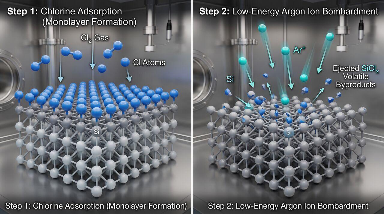
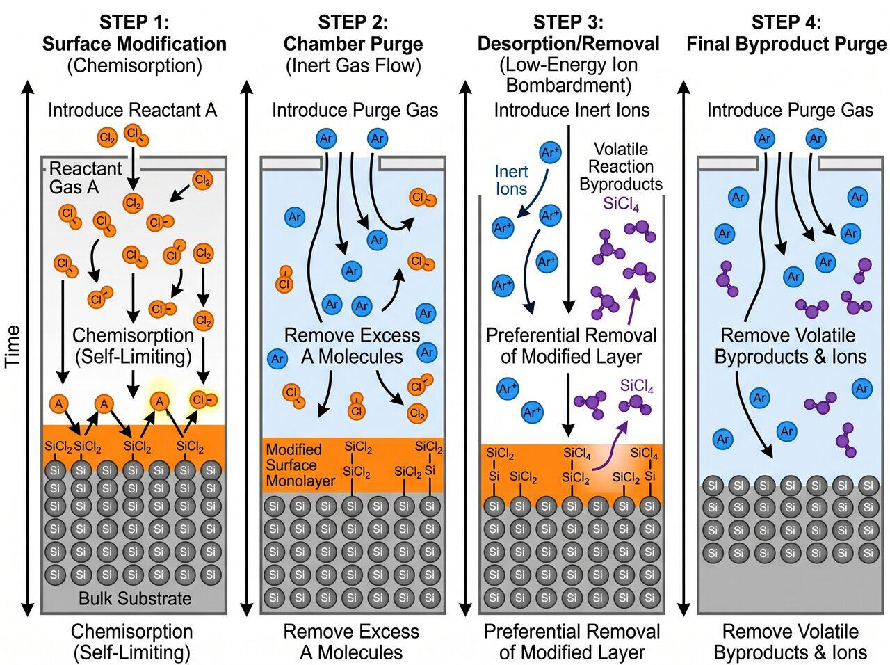
Every ALE process operates by splitting material removal into separate, self-limiting half-reactions:
Self-Limiting Behavior
- Step 1 (Modification): Adsorption terminates automatically once all available surface bonding sites are saturated.
- Step 3 (Removal): The removal energy is tuned strictly below the bulk material sputtering threshold. Once the modified top atomic monolayer is removed, etching stops completely, regardless of extended step duration.
03Directional vs. Thermal ALE
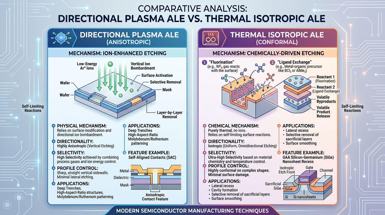
ALE processes fall into two main operational categories based on material requirements and feature geometries:
| Parameter | Directional Plasma ALE | Thermal Isotropic ALE |
|---|---|---|
| Removal Mechanism | Low-energy directional ion impact () | Ligand exchange or fluorination/complexation |
| Profile Control | Highly Anisotropic (Vertical 90°) | Isotropic (Conformal 360° removal) |
| Primary Materials | Silicon, Silicon Nitride (), Metals | High-k oxides (, ), Metals, Nitrides |
| Target Application | Self-Aligned Contacts (SAC), Nanosheet Spacer Etch | GAA Nanosheet Sacrificial Silicon-Germanium Release |
04Etch Per Cycle (EPC) & Synergy
The defining metric of ALE is Etch Per Cycle (EPC), typically expressed in Ångströms per cycle ():
Ideal ALE processes achieve synergy, ensuring that material removal occurs exclusively through the combined sequential cycle rather than unconditioned spontaneous etching.
→Prerequisites & continue reading
Prerequisites: ["p06-t6.1-t1-plasma-etching-rie-icp-ccp-fundamentals"]
Also in Topic 6.2, Atomic Layer Etching:
Tier 2 · ALE Tool Architecture: High-Speed Gas Pulsing, Fast-…Tier 3 · Directional Plasma vs. Thermal Isotropic ALE: Surfac…