01Plasma Sheath Dynamics & The Bohm Criterion
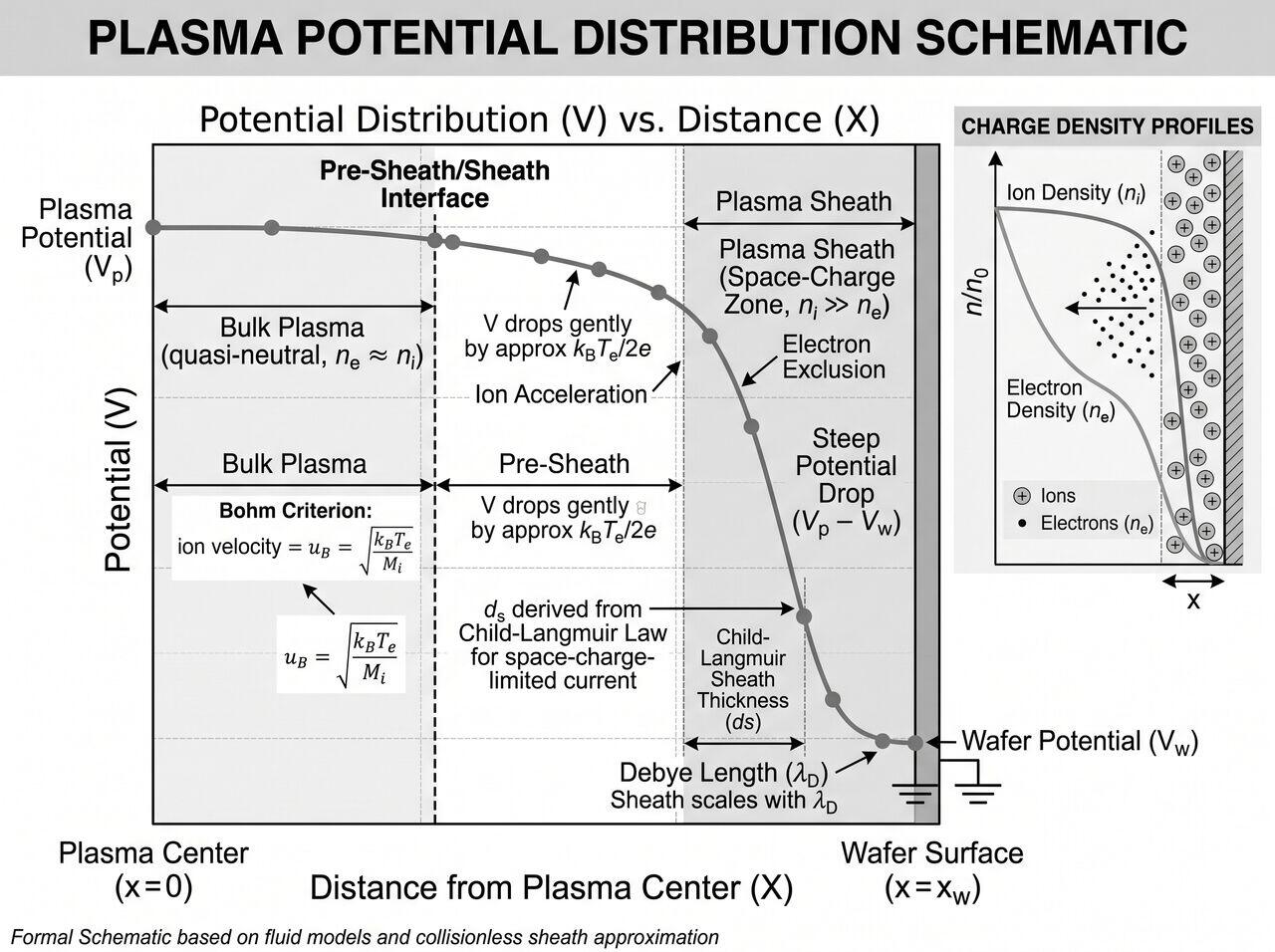
Because electrons have significantly higher thermal velocities than heavy positive ions (), an isolated substrate immersed in plasma rapidly acquires a negative electric potential relative to the bulk plasma. This potential repels electrons and attracts positive ions, creating a non-neutral positive space-charge boundary layer known as the Plasma Sheath.
The Bohm Criterion
For a stable, stationary sheath to form, positive ions entering the sheath edge from the bulk plasma must reach a critical minimum velocity, the Bohm Velocity ():
where is electron temperature, is Boltzmann's constant, and is ion mass. Ions are accelerated across a quasi-neutral "pre-sheath" region by a potential drop to satisfy this criterion before entering the high-voltage sheath.
Child-Langmuir Law for Collisionless Sheaths
The ion current density () traversing a collisionless sheath of thickness under a sheath DC self-bias potential follows the Space-Charge Limited Current equation:
This mathematical relationship dictates that increasing RF bias voltage expands the sheath thickness , altering ion transit times and ion energy distribution functions (IEDF).
02Thermochemical Surface Reaction Kinetics & Passivation
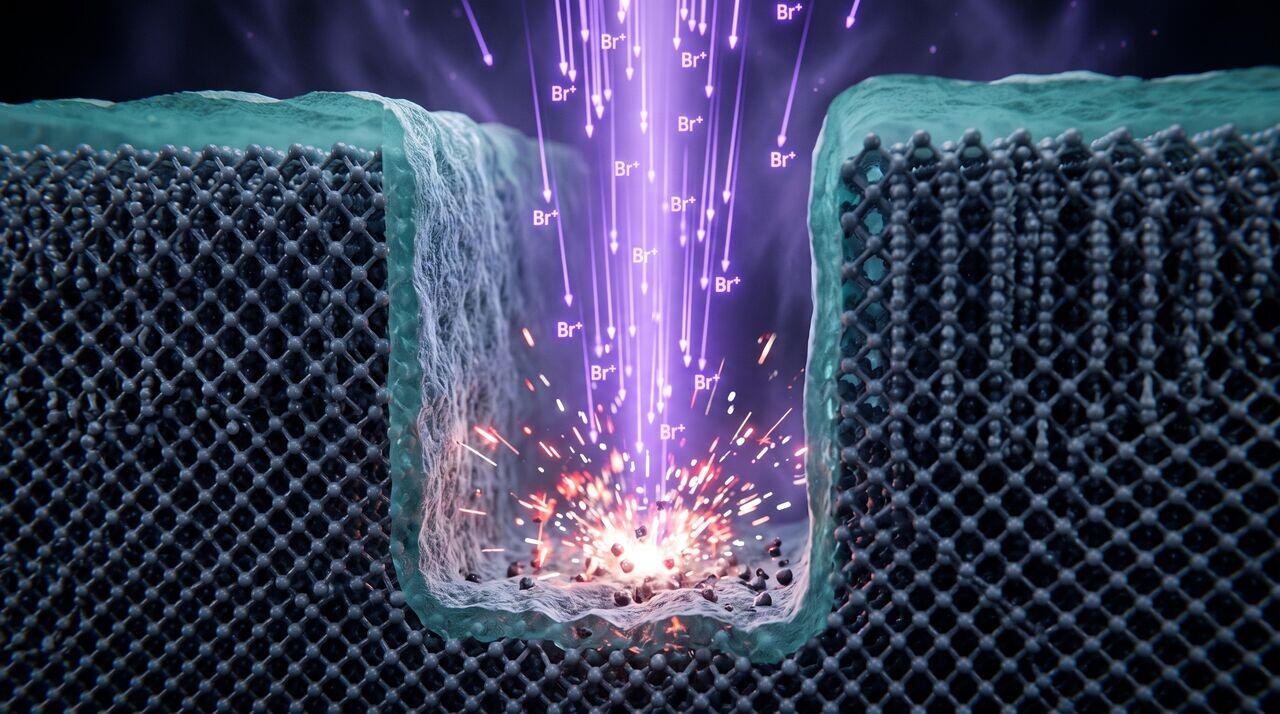
Anisotropic profile control in silicon gate etching relies on inhibitor-driven sidewall passivation. When etching silicon with chlorine/bromine chemistries (), the primary chemical reaction produces silicon tetrahalides:
- In-Situ Passivation Layer Generation: Oxygen additives react with etched silicon reaction products to deposit an ultrathin silicon oxyhalide passivation layer ( or ) on all exposed surfaces.
- Selective Removal: Directional ions continuously bombard the trench floor, sputtering away the passivation layer and exposing fresh silicon to chemical radicals.
- Sidewall Protection: Unbombarded vertical sidewalls retain the passivation film, preventing lateral etching and enabling vertical feature profiles with aspect ratios exceeding 50:1.
03Micro-loading, Aspect Ratio Dependent Etching (ARDE) & Profile Anomalies
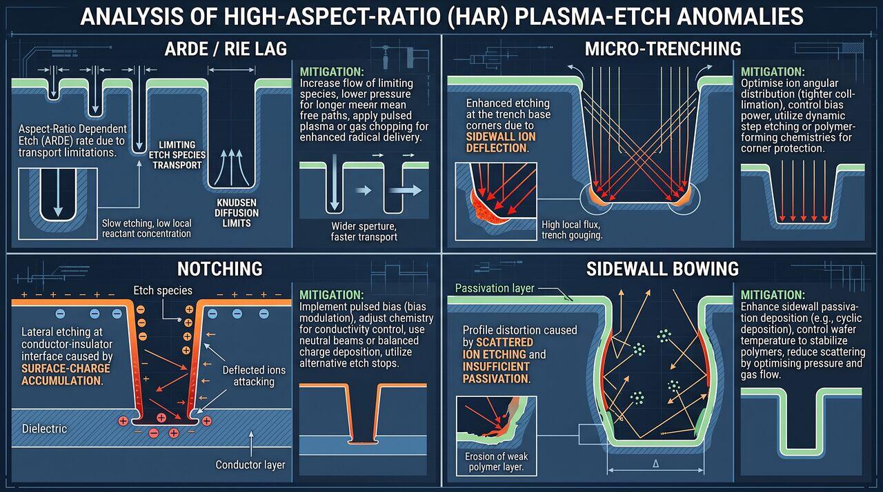
As features scale down, transport phenomena inside narrow trenches limit etch performance:
- Aspect Ratio Dependent Etching (ARDE / RIE Lag): Etch rates decrease as trench aspect ratios increase. Conductance limits Knudsen diffusion of neutral species to the trench bottom, while charging of insulating sidewalls deflects incoming ions.
- Micro-Trenching: Ions grazing against vertical sidewalls deflect toward the outer corners of the trench bottom, creating localized over-etch grooves.
- Notching: Charge separation at the bottom of insulating layers (e.g., STI trench stops) causes electron accumulation at feature tops and positive ion accumulation at the bottom, creating a lateral electric field that drives ions sideways, carving out notch defects.
→Prerequisites & continue reading
Prerequisites: ["p06-t6.1-t2-chamber-hardware-rf-bias-plasma-kinematics"]
Also in Topic 6.1, Reactive Ion Etching & Plasma Physics:
Tier 1 · Plasma Etching & Reactive Ion Etching (RIE): Core Fu…Tier 2 · ICP/CCP Etch Chamber Mechanics, Dual-Frequency RF Bi…