01What is High-Aspect-Ratio (HAR) Etching?
In semiconductor manufacturing, the Aspect Ratio (AR) of a feature is defined as the ratio of its depth (H) to its width or diameter (W):
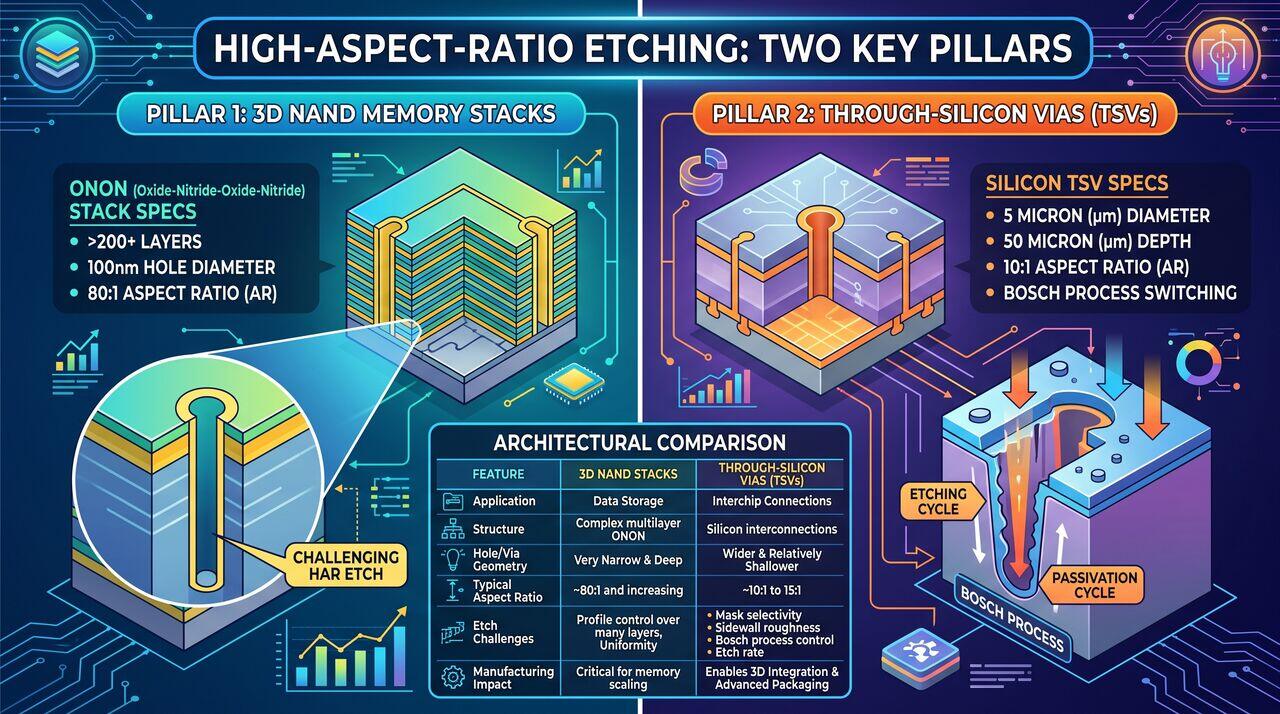
While standard planar CMOS processing deals with aspect ratios of 3:1 to 10:1, modern 3D architectures, specifically 3D NAND Flash Memory and Through-Silicon Vias (TSVs), require etching vertical channels with extreme aspect ratios exceeding 80:1 to 100:1.
02Primary Industrial Applications: 3D NAND & TSVs
- 3D NAND Channel Hole Etch: Modern 3D NAND flash devices stack over 200 to 300 alternating layers of silicon oxide () and silicon nitride () ONON memory stacks. A single plasma etch step must pierce through this thick stack to punch uniform wide memory channel holes from top to bottom.
- Through-Silicon Vias (TSV): In 2.5D/3D heterogeneous packaging, TSVs require etching deep vertical silicon vias ( wide by deep, ) to establish vertical electrical interconnections across stacked memory and logic dies.
03Fundamental Physical Obstacles in Deep Trenches
As a trench deepens, the plasma etch process experiences severe physical transport limitations:
PHYSICAL LIMITATIONS IN HAR TRENCHES
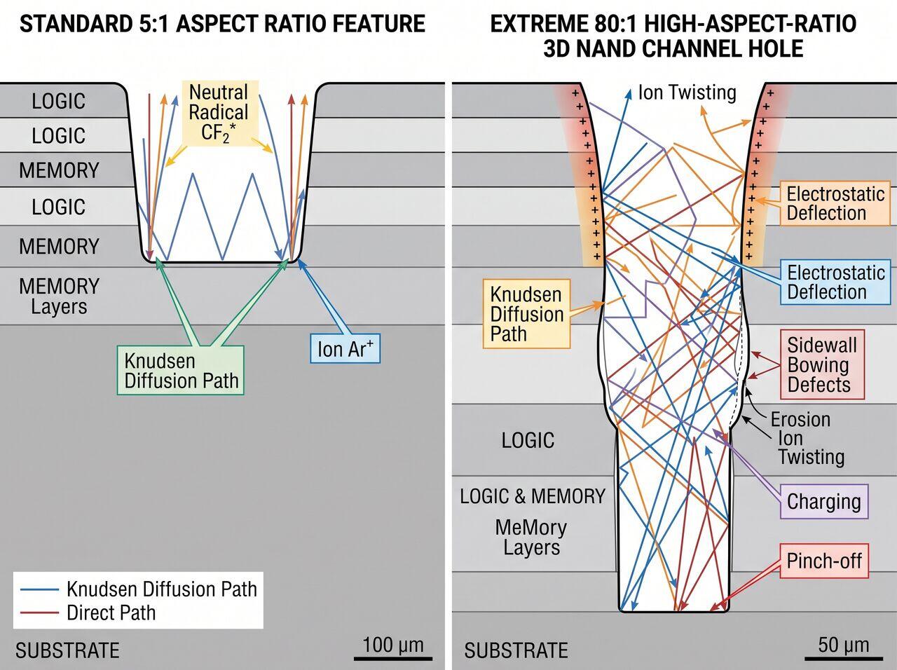
1. Neutral Radical Depletion (Knudsen Diffusion Limit)
2. Ion Angular Dispersion & Sidewall Charging Deflection
3. Reaction Byproduct Transport Blockade (Clogging)
- Knudsen Diffusion Resistance: At deep trench bottoms, gas molecules collide more frequently with trench walls than with each other, reducing neutral radical arrival flux by over .
- Sidewall Charging & Ion Deflection: Insulating oxide/nitride sidewalls accumulate positive charge from incoming ions, creating electrostatic repulsion that deflects subsequent ions into sidewalls, causing bowing and twisting.
- Byproduct Redeposition: Heavy non-volatile fluorocarbon etch byproducts become trapped at trench bottoms, blocking further chemical removal.
→Prerequisites & continue reading
Prerequisites: ["p06-t6.1-t1-plasma-etching-rie-icp-ccp-fundamentals"]
Also in Topic 6.3, High-Aspect-Ratio Plasma Etching:
Tier 2 · HAR Etcher Hardware: Cryogenic Sub-Zero Cooling & Hi…Tier 3 · Deep-Trench Ion Transport, ARDE Modeling, Striation …