01Executive Overview & Physical Intent
After photolithography defines a photoresist pattern on a wafer, plasma etching (specifically Reactive Ion Etching - RIE) is the primary subtractive process used to transfer that pattern into underlying materials, such as silicon, silicon dioxide (), silicon nitride (), or metals.
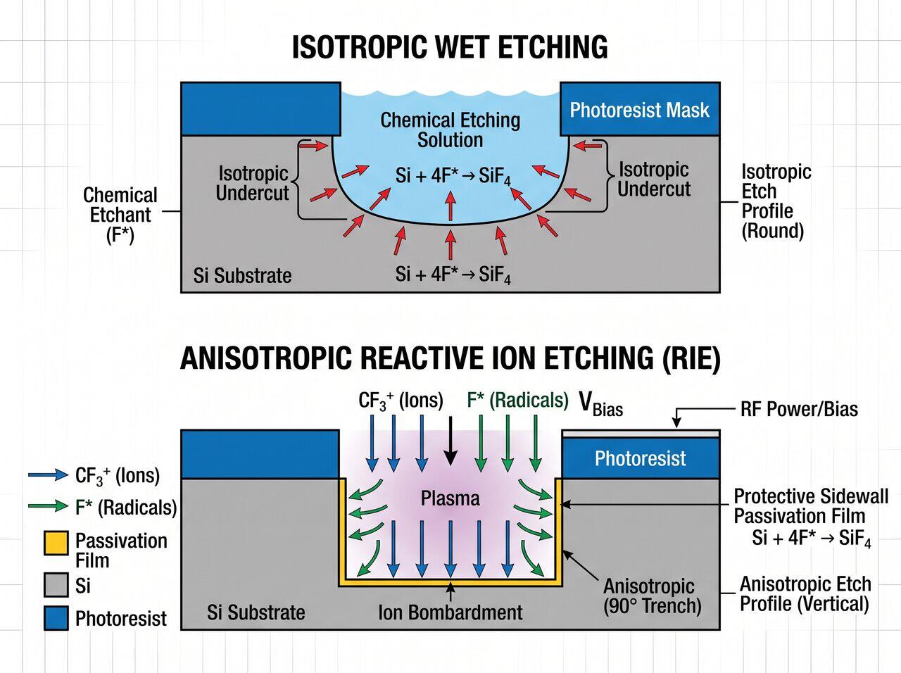
In early semiconductor manufacturing, wet chemical etching was used to dissolve exposed materials. However, wet etching is inherently isotropic, etching equally in all directions (both vertically and laterally under the mask). For sub-micron feature sizes, isotropic etching causes complete pattern undercutting, destroying narrow lines and features.
Plasma etching solves this challenge by combining chemical reactivity (reactive chemical radicals) with physical bombardment (energetic, directional ions). This synergy enables anisotropic etching, producing straight 90° vertical sidewalls with sub-nanometer directional control.
02Fundamental Process Mechanics: The Dual Mechanism
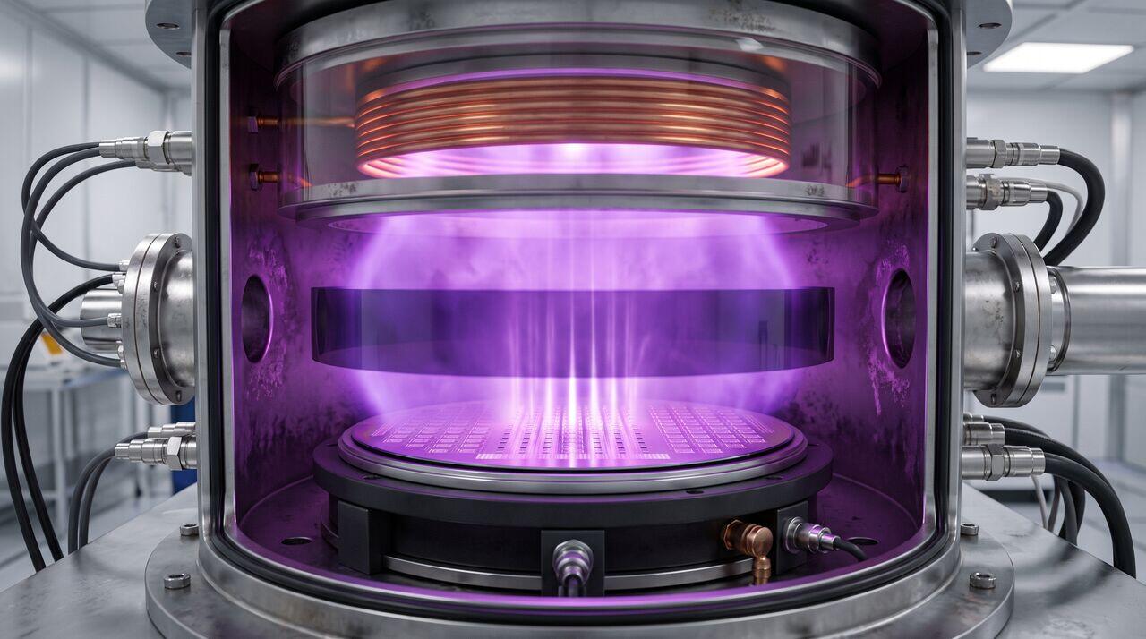
Reactive Ion Etching relies on a low-pressure radio-frequency (RF) plasma containing electrons, positive ions, neutral atoms, and highly reactive free radicals.
- Chemical Etching (Radical-Driven): Reactive gas species (such as fluorine radicals or chlorine radicals ) adsorb onto the exposed surface and chemically react with target atoms to form volatile byproducts (e.g., ). This chemical component is highly selective to the target material but inherently isotropic.
- Physical Etching (Ion-Driven): Positive ions (, ) are accelerated vertically toward the wafer by an electric bias across the plasma sheath. These ions physically sputter atoms and break chemical bonds on horizontal surfaces.
- Synergistic Anisotropic Removal: Physical ion impact selectively weakens bonds and removes protective passivation layers on horizontal trench bottoms, allowing chemical radicals to rapidly etch vertically while vertical sidewalls remain protected.
03High-Level Comparison of Plasma Architectures: CCP vs. ICP
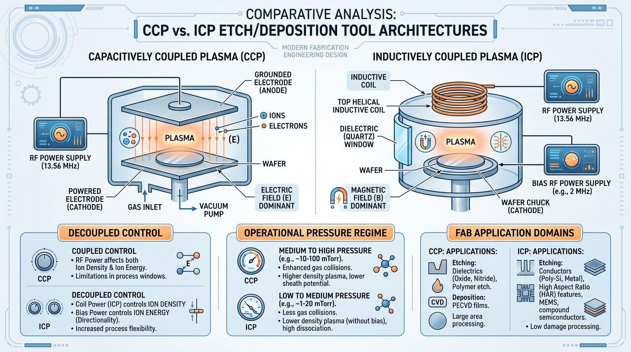
In modern fabs, plasma etching tools are divided into two major RF chamber configurations:
| Parameter / Feature | Capacitively Coupled Plasma (CCP) | Inductively Coupled Plasma (ICP) |
|---|---|---|
| RF Energy Coupling | Electrostatic (Parallel Plate Electrodes) | Electromagnetic (Inductive Coil Antenna) |
| Plasma Density | Low to Moderate () | High () |
| Ion Density vs. Energy Control | Coupled (Changing RF power alters both) | Decoupled (Separate Coil RF and Chuck Bias RF) |
| Primary Fab Applications | Dielectric etching (, Low-k, High-k), BEOL | Silicon trench etch, gate patterning, conductor etch |
04Key Performance Metrics in Fab Etch Operations
- Anisotropy (A): A measure of directional etch control, defined as , where is lateral etch rate and is vertical etch rate. Ideal anisotropic etching achieves .
- Etch Selectivity (S): The ratio of the etch rate of the target layer to the etch rate of the mask or underlying stop layer (). High selectivity prevents mask erosion and substrate gouging.
- Etch Uniformity: The percentage variation in etch depth across a wafer (typically controlled to 3-sigma).
→Prerequisites & continue reading
Prerequisites: ["p05-t5.1-t1-duv-immersion-193i-lithography-fundamentals"]
Also in Topic 6.1, Reactive Ion Etching & Plasma Physics:
Tier 2 · ICP/CCP Etch Chamber Mechanics, Dual-Frequency RF Bi…Tier 3 · Plasma Sheath Physics, Bohm Criterion & Sidewall Pas…