01Introduction: Polysilicon vs Monocrystalline Silicon
Electronic-Grade Polysilicon (EGS) produced by the Siemens process is pure, but it cannot be used directly to manufacture microchips. Why? Because polysilicon consists of millions of microscopic individual crystal grains oriented in random directions. The boundaries between these grains, called grain boundaries, act as electrical barriers that disrupt electron flow, trapping charges and rendering transistors unusable.
To build billions of identical nanoscale transistors on a wafer, the entire silicon substrate must consist of a single, continuous, perfectly ordered crystal lattice: a monocrystalline ingot (or single crystal).
02Method 1: The Czochralski (CZ) Growth Process
Over 95% of all silicon wafers used in microelectronics are produced using the Czochralski (CZ) method, invented by Polish scientist Jan Czochralski in 1916 and adapted for semiconductors in the 1950s.
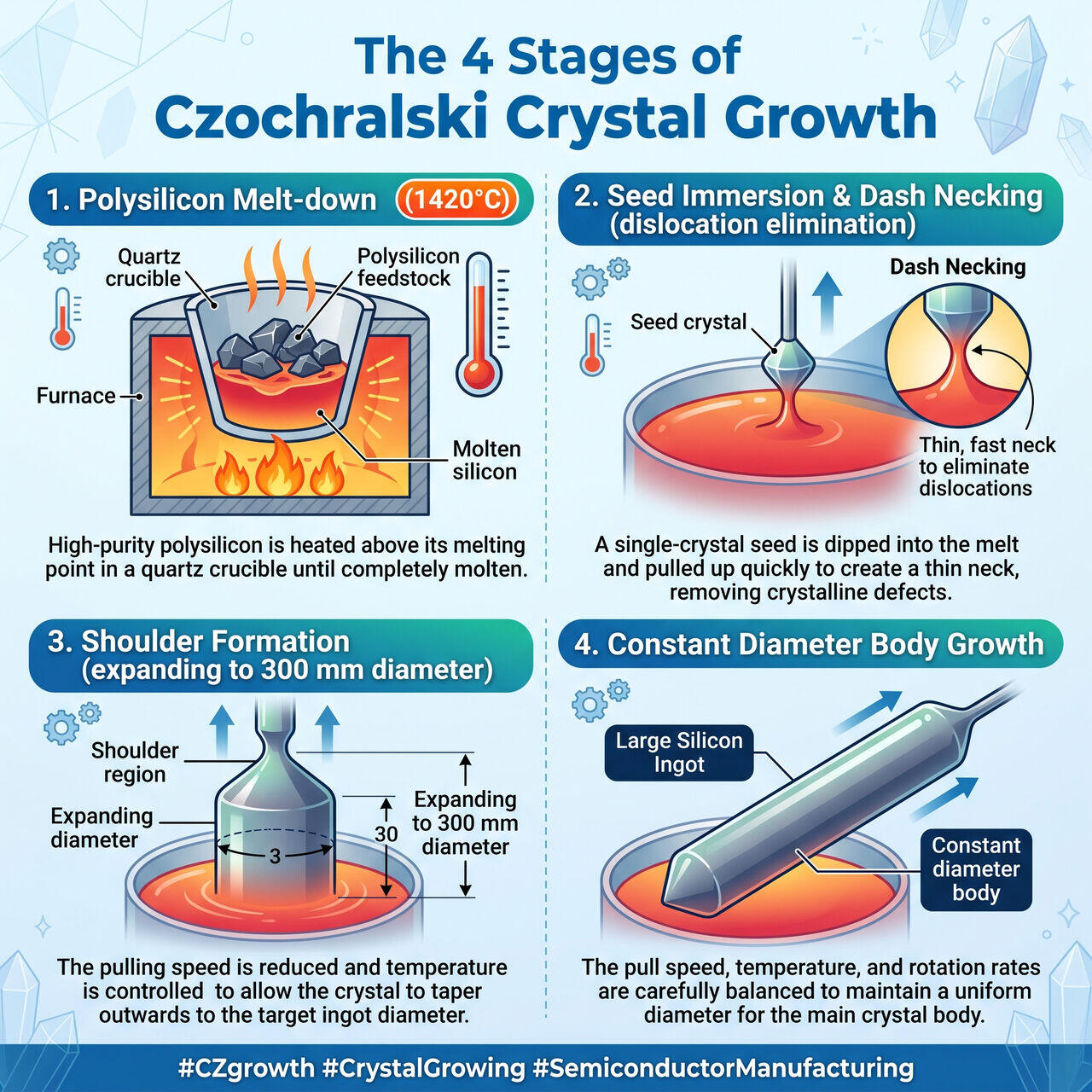
The 4 Stages of Czochralski Ingot Growth:
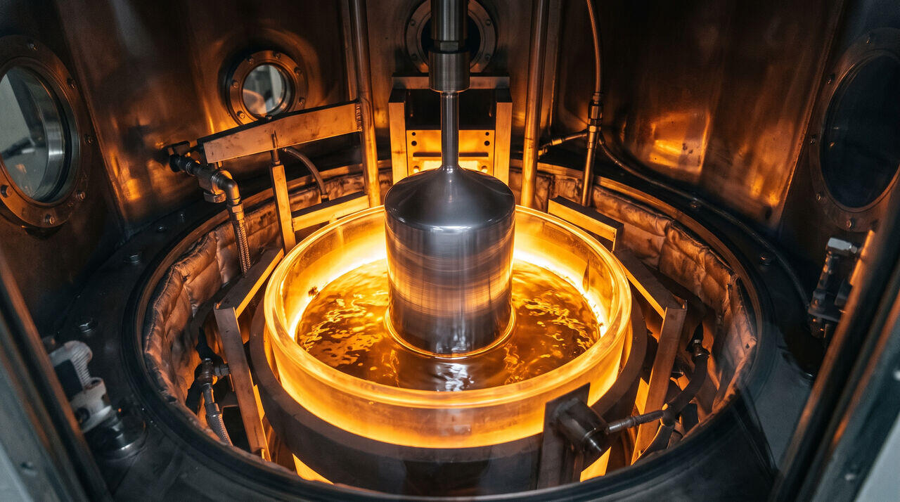
- Melting: Highly purified EGS polysilicon chunks are loaded into a high-purity quartz () crucible inside an argon-purged furnace and heated to (just above silicon's melting point of ).
- Seeding: A small, flawless single-crystal "seed" with a specific crystallographic orientation (typically or ) is dipped into the surface of the molten silicon.
- Dash Necking: The seed is rapidly pulled upward to form a thin "neck" ( in diameter, long). This critical step allows dislocations (crystal structure defects caused by thermal shock) to grow out to the edge and disappear, leaving a dislocation-free crystal.
- Shoulder & Body Growth: Pull speed and temperature are gradually adjusted to expand the crystal diameter to its target dimension (e.g., , or 12 inches) and pull a cylindrical body up to long weighing over .
03Method 2: The Float-Zone (FZ) Process
While the CZ method dominates digital logic and memory, high-voltage power electronics (like electric vehicle inverters and high-voltage grid converters) require silicon with extremely low oxygen content and ultra-high electrical resistivity (). Quartz crucibles in CZ furnaces leach trace oxygen into the melt, preventing high resistivity.
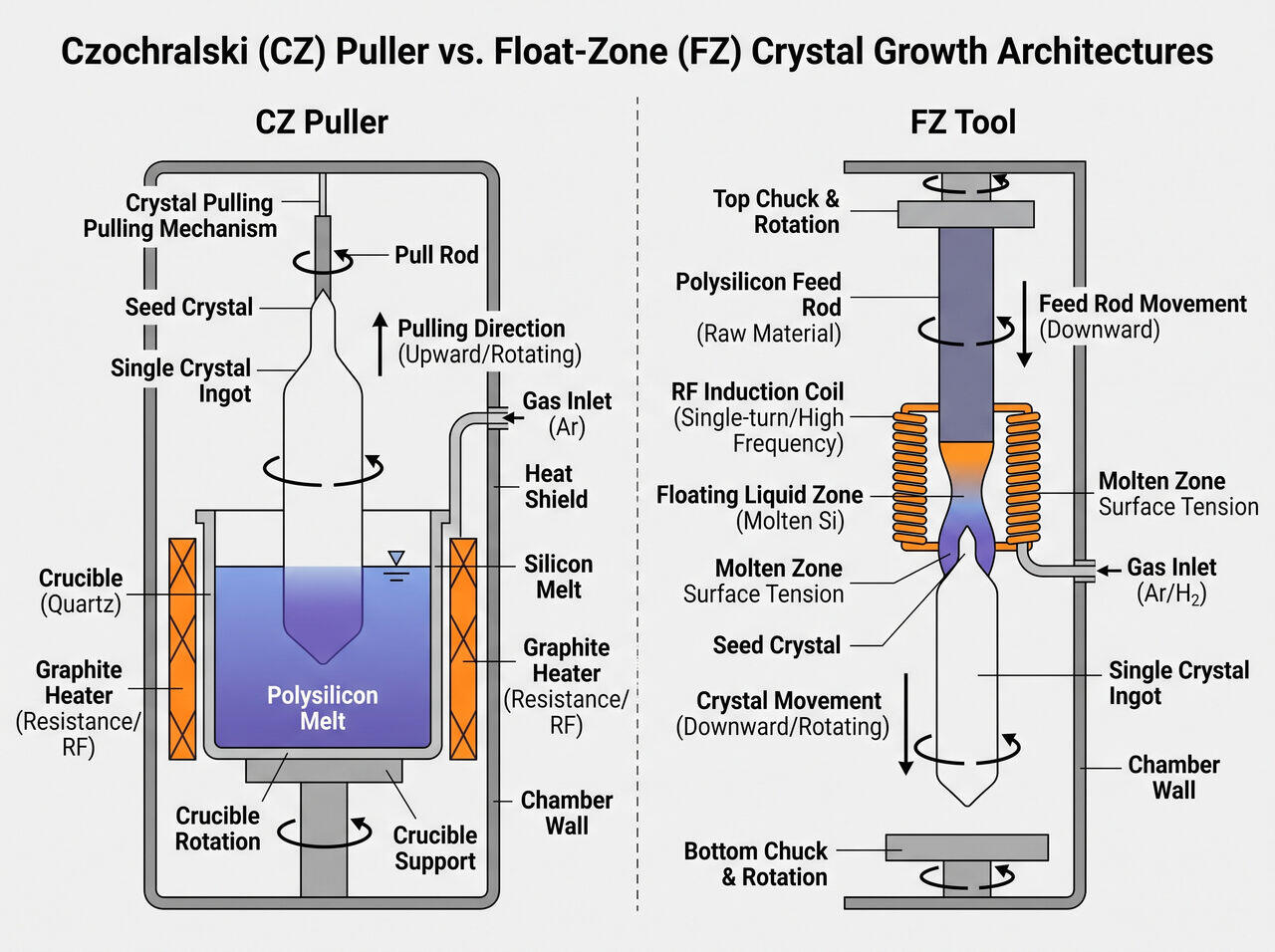
To solve this, the Float-Zone (FZ) method grows single crystals without using a crucible.
In FZ growth, a solid polysilicon rod is held vertically. A high-frequency Radio-Frequency (RF) induction coil surrounds a narrow band of the rod, melting a localized "floating zone" of silicon held together purely by surface tension. As the RF coil slowly moves upward along the rod, liquid silicon freezes onto a single-crystal seed below, leaving behind an ultra-pure crystal completely free of crucible oxygen contamination.
04CZ vs FZ Comparison Matrix
| Property / Parameter | Czochralski (CZ) Method | Float-Zone (FZ) Method |
|---|---|---|
| Crucible Material | Quartz () crucible used. | Crucible-free (RF induction coil). |
| Wafer Diameter Capacity | Up to ( demonstrated). | Limited to due to surface tension limits. |
| Oxygen Content | High (). | Ultra-Low (). |
| Manufacturing Cost | Lower cost; high throughput. | Higher cost; complex vertical motion control. |
| Primary Industry Use | Microprocessors, AI Chips, DRAM, NAND Flash. | Power MOSFETs, IGBTs, High-Voltage Thyristors. |
05Key Takeaways & Summary
- Monocrystalline Necessity: Transistors require a single continuous crystal structure; grain boundaries in polysilicon degrade electrical performance.
- CZ Method: Dominates 95%+ of industry. Uses a seed crystal dipped into molten silicon inside a quartz crucible to pull ingots.
- Dash Necking: A thin neck is grown first to eliminate line defects (dislocations) before expanding the ingot diameter.
- FZ Method: Crucible-free method using RF melting for ultra-pure power semiconductor substrates.
→Prerequisites & continue reading
Prerequisites: Understanding of EGS polysilicon production (Topic 1.2) and basic crystal lattices
Also in Topic 1.3, Monocrystalline Growth: Czochralski & Float Zone:
Tier 2 · Czochralski Crystal Pullers and CUSP Magnetic Field …Tier 3 · Voronkov Criterion (v/G), Microdefect Control, and O…