01Intrinsic Point Defect Thermodynamics at Solidification
During the solidification of silicon at its melting point (), the crystal lattice incorporates intrinsic point defects: vacancies (V, missing silicon atoms) and self-interstitials (I, extra silicon atoms squeezed between lattice sites).
At high temperatures, both species exist in dynamic equilibrium. As the growing crystal cools below the solidus interface, these point defects recombine (). The species present in higher concentration after recombination dictates the microdefect regime of the entire wafer.
02The Voronkov Criterion: The v/G Ratio
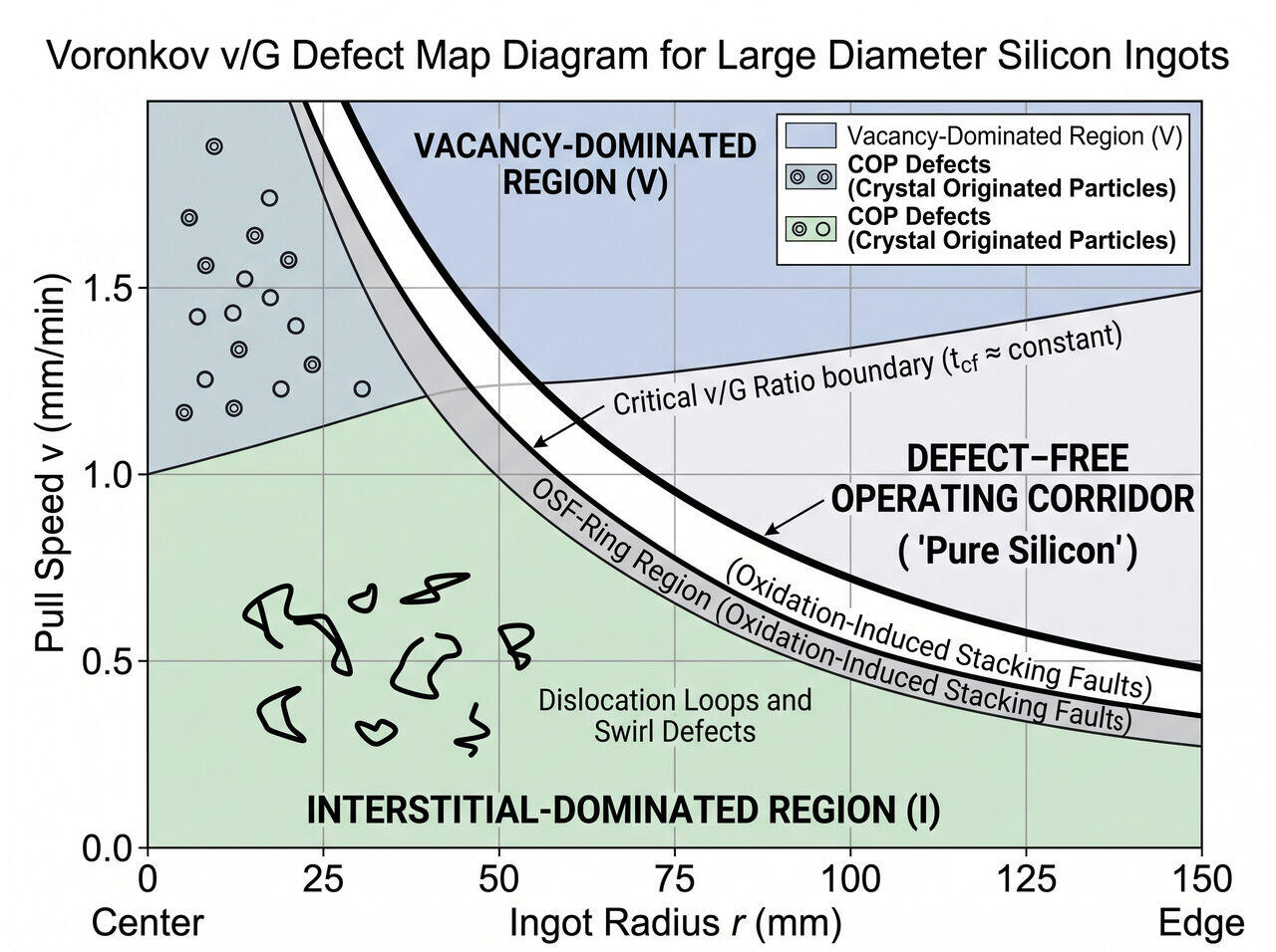
In 1982, V.V. Voronkov established the fundamental mathematical framework governing point defect incorporation in single-crystal silicon. The incorporated defect type is determined by the ratio of pull speed (v, in ) to axial temperature gradient (G, in ):
The Critical Threshold ()
- Critical Value: (depending on exact thermal conditions).
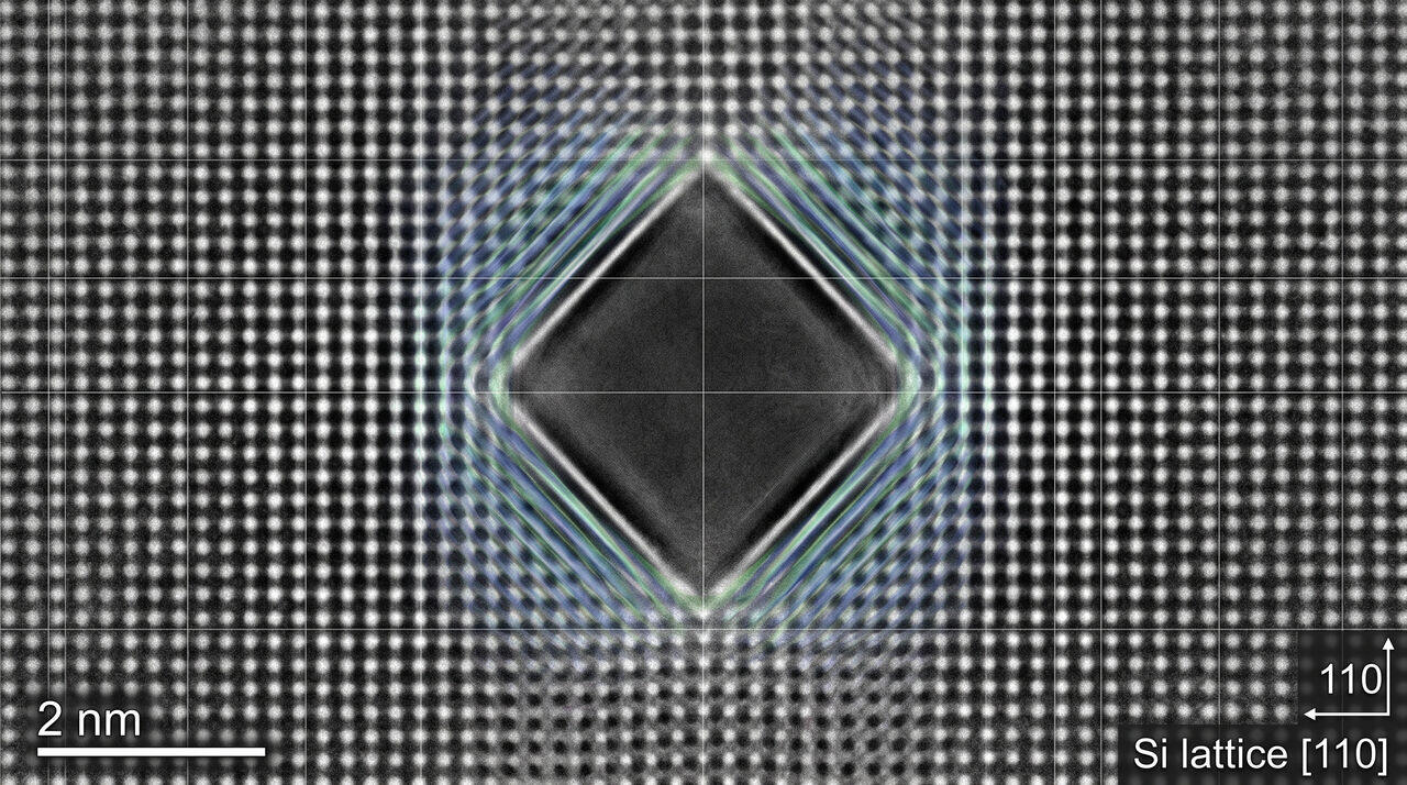
- If : Vacancy diffusion dominates. Excess vacancies recombine during cooling to form microscopic octahedral voids ( in size) known as Crystal-Originated Particles (COPs). When sliced into wafers, COPs create surface pits that destroy transistor gate oxide integrity.
- If : Self-interstitial diffusion dominates. Excess interstitials aggregate into large dislocation loops and interstitial clusters (A-swirl defects), causing catastrophic electrical leakage across transistor junctions.
The Goal: Perfect "Pure Silicon" ( Regions)
By precisely engineering thermal shields inside the furnace to maintain a uniform spatial G(r) across the ingot radius, crystal pullers operate exactly at , producing defect-free monocrystalline silicon.
03Oxygen Incorporation Kinetics and Thermal History
Oxygen is an inevitable chemical species in Czochralski silicon due to the dissolution of the quartz () crucible wall by molten silicon:
Dissolved oxygen is transported by melt convection to the growth interface, incorporating interstitially () into the silicon lattice at concentration levels between and .
Thermal Donors and Oxygen Precipitation Dynamics
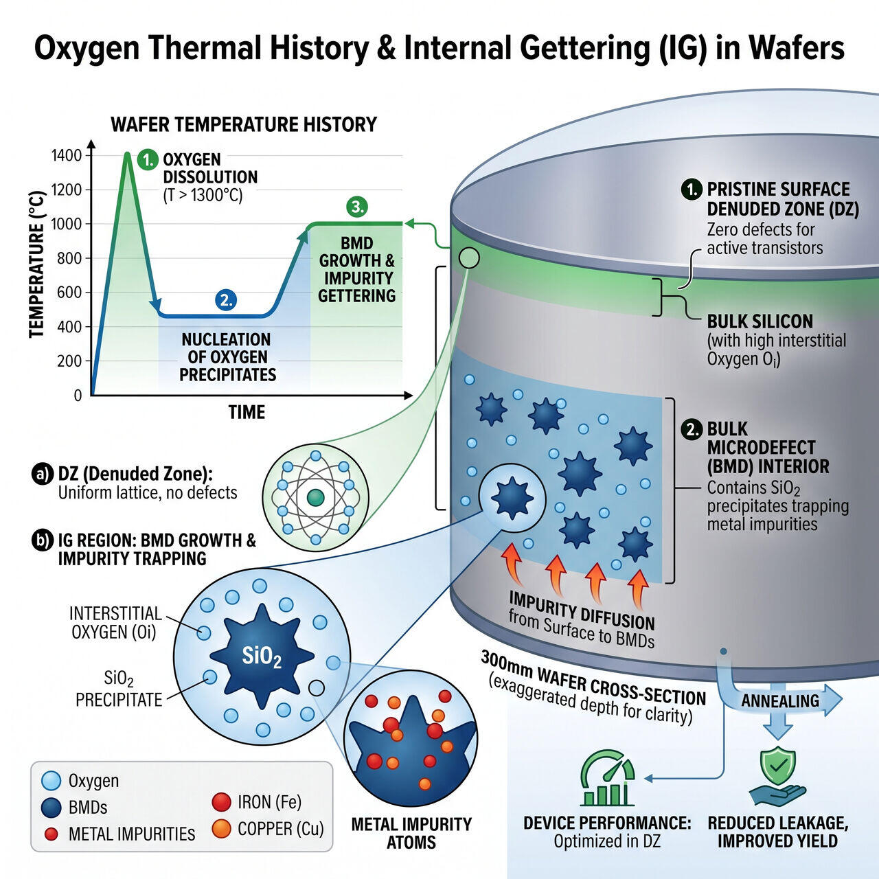
- Thermal Donor Formation ( Window): As the ingot slowly cools through the thermal window, interstitial oxygen atoms aggregate into small clusters (), which act as electrical double-donors. Thermal donors alter the intended electrical resistivity of the wafer and must be destroyed by high-temperature rapid thermal annealing ( for ).
- Internal Gettering (IG) Engineering: Controlled oxygen precipitation is utilized intentionally for Internal Gettering (IG). High-temperature furnace cycles form microscopic precipitates in the bulk interior (bulk microdefects, BMDs) while leaving a pristine, defect-free "denuded zone" (DZ) at the top surface where transistors are built. The bulk precipitates act as internal traps, capturing mobile metallic contaminants () away from surface transistors.
04Mathematical Model of Point Defect Transport
The steady-state radial and axial distribution of vacancies () and interstitials () is governed by the coupled advection-diffusion-recombination differential equations:
Where:
- v is crystal pull speed.
- are species diffusion coefficients.
- is the vacancy-interstitial recombination rate constant.
- are thermal equilibrium defect concentrations.
Numerical finite-element simulation of these equations allows crystal growth engineers to design complex thermal hot-zones that maintain v/G(r) within the defect-free window across the entire wafer radius.
→Prerequisites & continue reading
Prerequisites: Advanced crystal defect thermodynamics, point defect kinetics, heat transfer modeling
Also in Topic 1.3, Monocrystalline Growth: Czochralski & Float Zone:
Tier 1 · Growing the Perfect Single Crystal: Czochralski and …Tier 2 · Czochralski Crystal Pullers and CUSP Magnetic Field …