01Introduction: Transforming As-Sliced Wafers into Fab-Ready Substrates
When silicon wafers emerge from multi-wire diamond sawing, they are disk-shaped and roughly thick, but they are far from usable for semiconductor chip fabrication.
Freshly sliced "as-sliced" wafers suffer from four major mechanical flaws:
- Sharp, Fragile Edges: The perimeter of the wafer has sharp right-angle corners that chip extremely easily during robotic transfer.
- Thickness Irregularity & Saw Marks: Both front and back surfaces exhibit parallel micro-grooves (saw marks) and thickness variations ().
- Deep Subsurface Damage (SSD): Microcracks extend deep into the silicon crystal lattice on both sides.
- Residual Mechanical Stress: Slicing leaves high internal mechanical stress that distorts the wafer lattice.
To eliminate these defects, every wafer passes through three critical surface conditioning steps before Chemical Mechanical Polishing (CMP): Edge Profiling (Grinding), Double-Side Lapping, and Chemical Stress-Relief Etching.
02Step 1: Wafer Edge Profiling (Beveling)
Why Edge Profiling is Necessary
If a wafer retains sharp edges, robotic handling claws in automated fab tools will cause micro-chipping at the wafer perimeter. Silicon chips floating inside processing chambers create catastrophic particle contamination that destroys IC yields! Furthermore, film stress during high-temperature CVD deposition causes films to peel off sharp corners.
How Edge Profiling Works
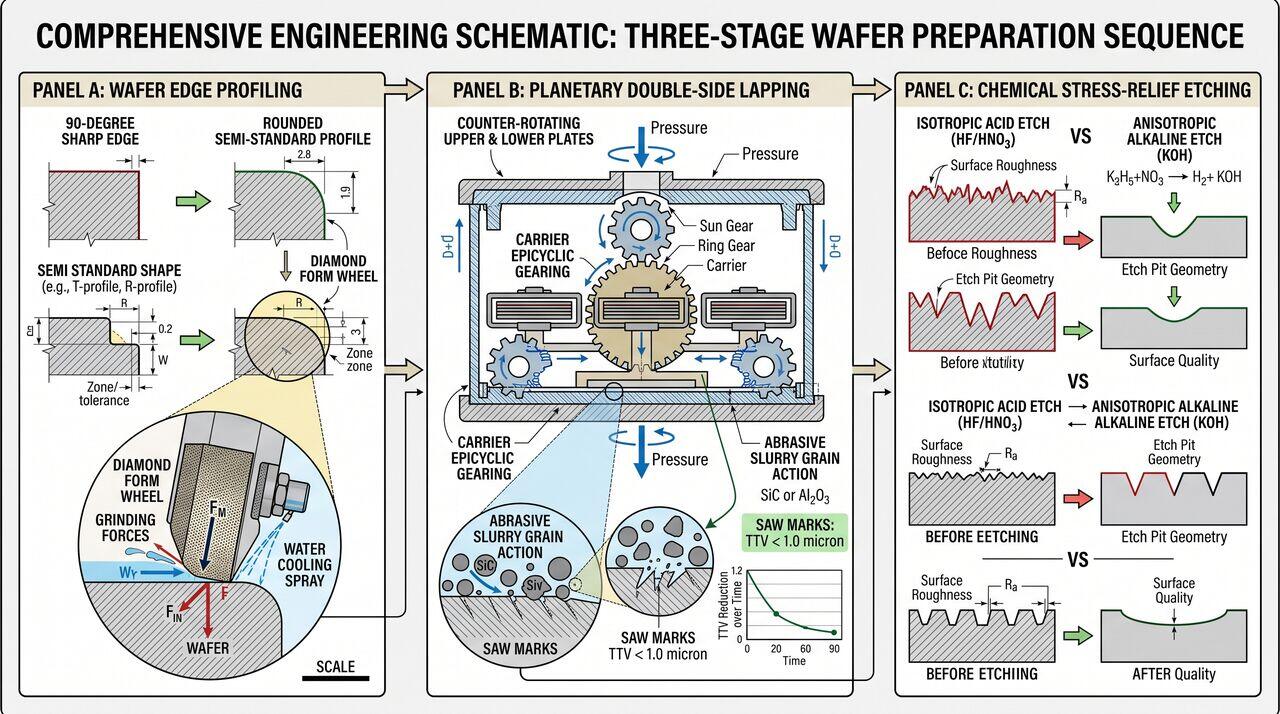
The wafer is mounted on a high-speed vacuum chuck and rotated against a diamond-impregnated CNC form-grinding wheel. The wheel profile shapes the wafer edge into a smooth, rounded, bullet-nose contour compliant with SEMI standards.
03Step 2: Double-Side Lapping (Planarization)
Purpose of Lapping
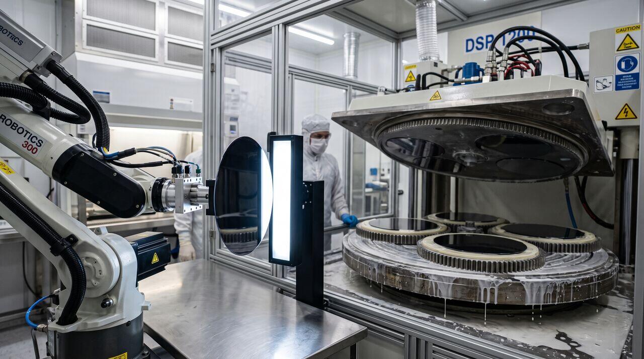
Multi-wire sawing leaves wire marks and thickness variations across the wafer. Double-Side Lapping is a batch mechanical abrasive process designed to flatten both sides of the wafer simultaneously, achieving extreme thickness uniformity ().
Lapping Mechanics
- Planetary Carrier System: Multiple wafers are placed inside circular fiberglass or steel "carrier gears" held between two massive, counter-rotating cast-iron lapping plates.
- Abrasive Slurry: A liquid slurry containing alumina () or boron carbide () grains ( size) suspended in glycerine or water is pumped between the plates.
- Dual Action: As the plates rotate under pressure, the abrasive grains roll and slide over both wafer surfaces simultaneously, abrading away high spots, removing saw marks, and producing flat, parallel wafer surfaces.
04Step 3: Chemical Stress-Relief Etching
Lapping achieves excellent flatness (), but because it is a mechanical grinding process, it leaves a new, uniform layer of fine subsurface damage ( deep) on both sides of the wafer.
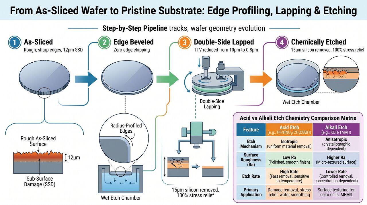
Chemical Stress-Relief Etching is an isotropic wet chemical process that dissolves this damaged surface layer without applying any mechanical force, revealing pristine, stress-free single-crystal silicon.
Acid Etching vs. Alkali Etching
There are two primary chemical etching formulations used in commercial silicon manufacturing:
| Parameter | Acidic Etching () | Alkaline Etching () |
|---|---|---|
| Etch Mechanism | Isotropic chemical oxidation and dissolution | Anisotropic crystallographic dissolution |
| Surface Morphology | Ultra-smooth, rounded waviness ("orange peel") | Faceted micro-textures (cleavage planes) |
| Etch Rate | High rate () | Moderate rate () |
| Waviness / Flatness | Preserves long-range flatness well | Can degrade local flatness on wafers |
| Safety & Environment | High NO fumes; complex bath control | Safer, easier effluent neutralisation |
Modern wafer manufacturing lines frequently employ a mixed or two-step etching sequence (alkaline etching followed by a mild acidic polish etch) to combine high throughput with superior surface waviness control.
05Summary & Next Steps in the Fab
Together, Edge Profiling, Double-Side Lapping, and Stress-Relief Etching transform rough, fragile as-sliced wafers into:
- Smoothly beveled, chip-resistant substrates.
- Ultra-flat parallel disks with Total Thickness Variation .
- Stress-free, pristine crystalline surfaces devoid of subsurface damage cracks.
With these mechanical and chemical preparation phases complete, the silicon wafers are ready for the final surface perfection stage: Chemical Mechanical Polishing (CMP), which produces mirror-finish surfaces with atomic-scale smoothness ().
→Prerequisites & continue reading
Prerequisites: Multi-Wire Diamond Sawing Fundamentals (Topic 2.2)
Also in Topic 2.3, Edge Profiling, Lapping & Stress-Relief Etching:
Tier 2 · Lapping & Etching Kinematics: Planetary Carrier Dyna…Tier 3 · Physics of Lapping & Etching: Tribochemistry, Anisot…