01Executive Summary & Microscopic Material Removal Physics
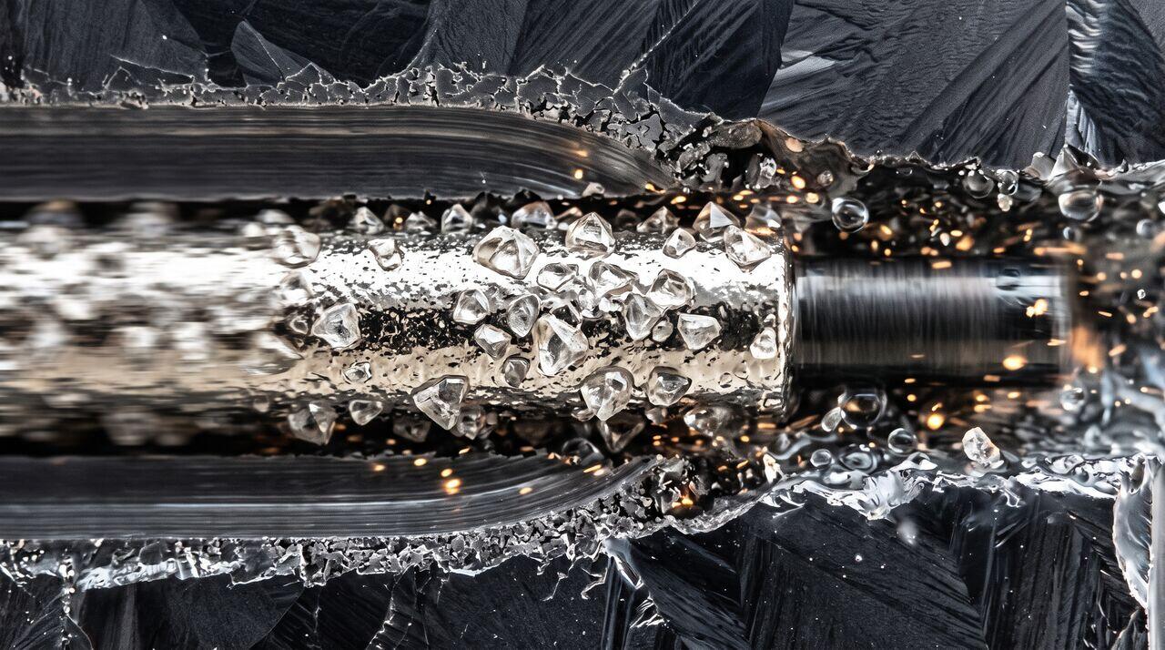
Slicing single-crystal silicon via Fixed Diamond Wire (FDW) sawing is fundamentally a high-velocity abrasive micro-scratching process. Unlike conventional grinding where abrasives are held in a rigid matrix, wire sawing involves diamond abrasive grains nickel-plated onto a flexible, high-tensile steel wire subject to non-linear elastic deflection, axial vibration, and hydrodynamic coolant resistance.
Material removal occurs as individual diamond grains protruding from the moving wire penetrate the silicon surface under vertical feed load:
- Ductile Micro-Ploughing: At low penetration depths, diamond grains create plastic deformation tracks via high-pressure solid-state phase transformation (Si-I to Si-II).
- Brittle Micro-Fracture: As local contact force exceeds critical indentation thresholds, lateral and median cracks form. Lateral crack overlap drives material detachment (chip formation), while median cracks extend downward into the substrate, dictating the Subsurface Damage (SSD) depth of the freshly sliced wafer.
02Quantitative Model of Wire Bow Dynamics & Slicing Force Balance
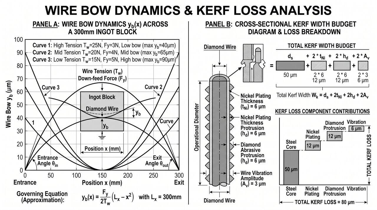
When the silicon ingot feeds downward into the moving wire web at rate , the flexible wire bends, creating a dynamic curve characterized by the Wire Bow Angle () and Wire Bow Height ().
Governing Differential Equation of Elastic Wire Bow
Modeling the wire as a flexible cable under axial tension subject to a uniform vertical cutting force distribution yields:
Assuming a uniform cutting force across ingot length L, integrating twice with boundary conditions and gives the parabolic bow profile:
The Maximum Wire Bow Height () occurring at the center of the ingot () is:
And the corresponding Wire Bow Angle () at the entry/exit points is:
Physical Implications of Wire Bow Physics
- Entrance and Exit Artifacts: Because varies along the cut length, the wire enters and exits the silicon block at an angle, creating geometric thickness deviations at the top and bottom edges of the wafer.
- Transient Ingot Entry/Exit: When the wire web first touches the top of the ingot block and when it breaks through the bottom, the contact length L(t) changes rapidly, causing non-steady-state wire bow variations that generate edge Warp and TTV defects.
03Kerf Loss Optimization & Wire Core Thinning Limits
Kerf Loss () represents the total width of silicon destroyed during slicing:
Where:
- = Diameter of the high-tensile steel wire core ().
- = Thickness of the electroplated nickel layer ().
- = Effective protrusion height of diamond abrasives ().
- = Transverse vibration amplitude of the moving wire ().
The Material Yield Equation
From a long silicon ingot, the maximum theoretical number of sliced wafers () is governed by wafer thickness () and kerf loss ():
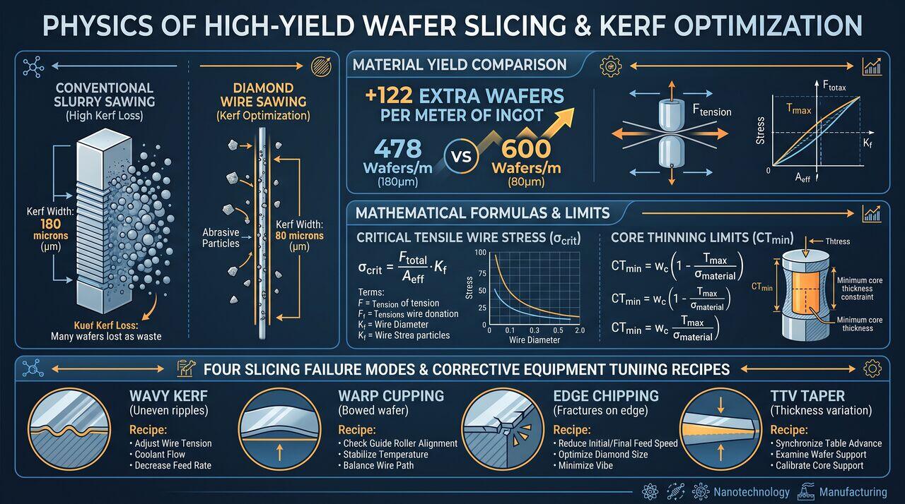
- Legacy Slurry Sawing (): .
- Advanced Diamond Wire (): .
- Yield Gain: ( increase in substrate production yield!).
Physical Limits of Wire Core Thinning
To reduce kerf loss further toward , core diameter () must drop below . However, tensile stress () within the steel wire core increases inversely with core cross-sectional area:
For and :
This stress approaches the ultimate tensile strength of ultra-high-carbon steel piano wire (), setting a hard physical limit on wire core thinning unless alternative ultra-high-strength core materials (such as carbon nanotube composite fibers or tungsten wires) are adopted.
04Subsurface Damage (SSD) Kinematics in Diamond Wire Slicing
Subsurface Damage produced during FDW slicing consists of surface microcracks, dislocation networks, and amorphous phase tracks extending into the bulk wafer.
SSD Depth Dependency Model
The maximum SSD depth () during fixed diamond wire sawing depends on diamond grain size (), wire speed (), feed rate (), and wire tension ():
Key Engineering Inferences:
- Higher Wire Speed () Reduces SSD: Operating at distributes the down-feed load across more diamond grains per second, reducing individual grain normal force () and decreasing median crack depth.
- Smaller Diamond Grit Reduces SSD: Transitioning from diamond grit to grit cuts maximum SSD depth from down to .
- Implications for Downstream Lapping: Lower initial slicing SSD allows lapping and chemical etching stock removal allowances to be reduced from down to , reducing chemical chemical waste and processing time.
05Yield Loss Mechanisms & Root Cause Failure Analysis
→Prerequisites & continue reading
Prerequisites: Wire Saw Machine Kinematics (Tier 2), Fracture Mechanics & Elasticity Theory
Also in Topic 2.2, Multi-Wire Diamond Sawing & Wafer Slicing:
Tier 1 · Multi-Wire Diamond Sawing Fundamentals: How Ingot Bl…Tier 2 · Wire Saw Machine Kinematics: Guide Roller Dynamics, …