01Introduction: The Challenge of Precision Wafer Slicing
Once a single-crystal silicon ingot has been cropped, ground to an exact cylinder, and notched for crystallographic orientation, it must be sliced into ultra-thin, flat wafers. This is one of the most mechanically demanding phases in semiconductor manufacturing.
Imagine taking a solid, extremely brittle cylinder of silicon, (12 inches) in diameter and over long, and slicing it into thousands of disk-shaped wafers, each only 775 micrometers () thick, without breaking a single one!
Historically, wafers were sliced one by one using Inner Diameter (ID) saw blades, a slow, expensive method that resulted in high material waste. Today, the global semiconductor industry exclusively uses Multi-Wire Diamond Sawing (MWDS), a high-throughput technology capable of slicing an entire silicon block into 2,000+ wafers simultaneously in a single processing run!
02Anatomy of a Multi-Wire Sawing Machine
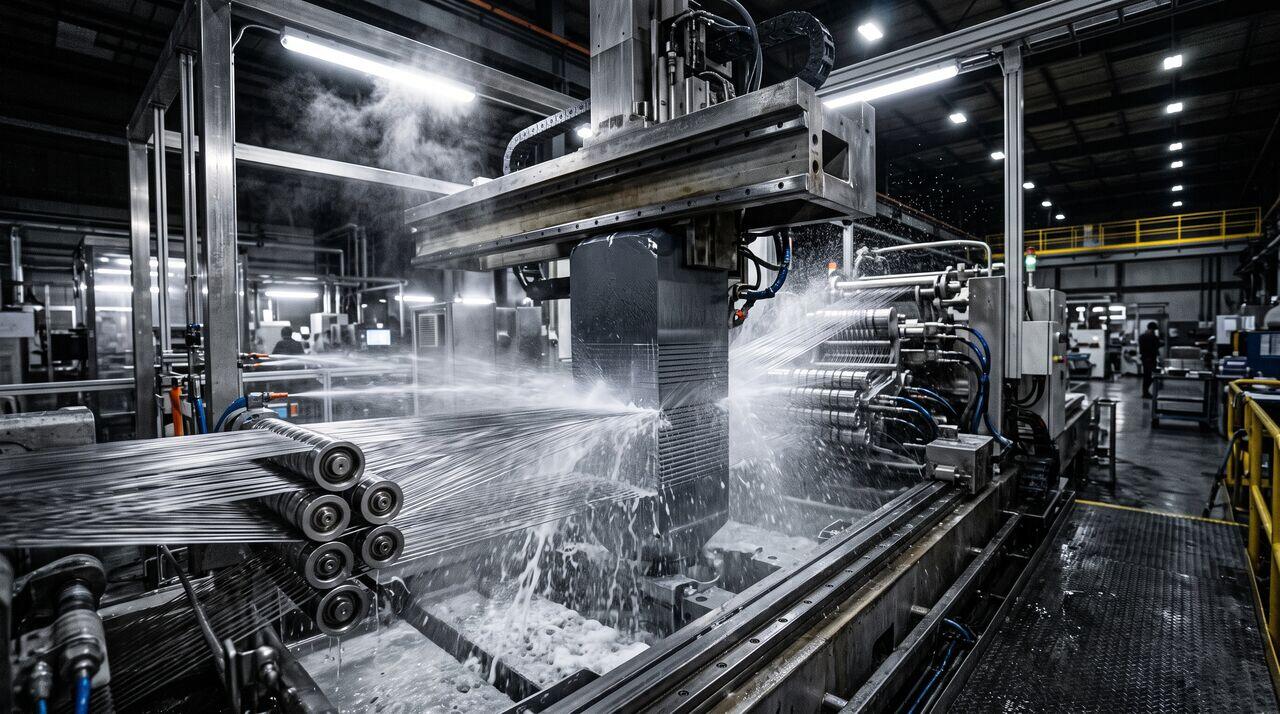
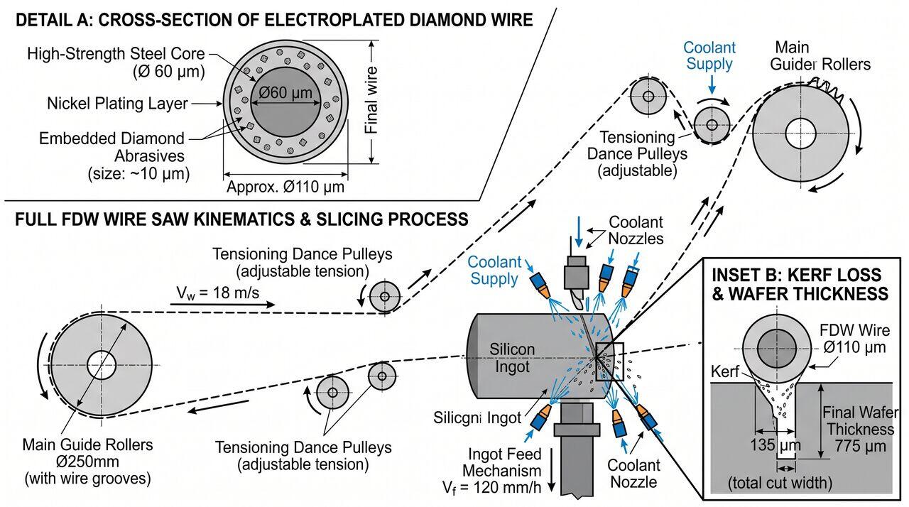
A modern multi-wire saw operates by forming a high-tension "web" of ultra-thin steel wire moving at speeds up to ().
Key Components of the Wire Saw Workcell
- The Wire Web: A single, continuous strand of steel wire, hundreds of kilometers long, is wound continuously around grooved polyurethane guide rollers (wire guides) to create a grid of thousands of parallel wire segments spaced less than apart.
- Fixed Diamond Wire: The steel wire (typically in core diameter) is permanently embedded with millions of microscopic industrial diamond particles ( grit) bonded via an electroplated nickel matrix.
- Ingot Feed Table: The silicon ingot block is glued to a sacrificial beam mounting plate and slowly pushed downward into the rapidly moving wire web.
- Coolant System: A continuous spray of water-based coolant flushes away fine silicon swarf and dissipates intense friction heat generated at the cutting interface.
03Free Abrasive Slurry vs. Fixed Diamond Wire (Technology Shift)
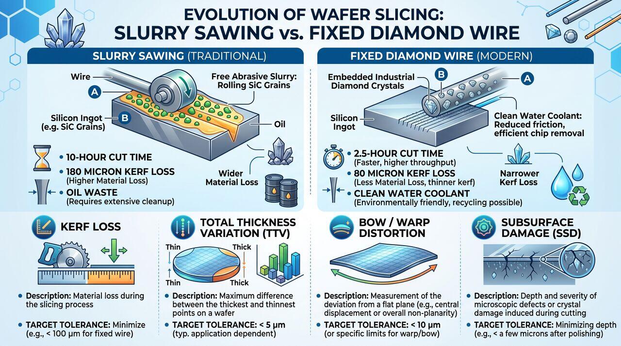
The industry underwent a major technological evolution from Free Abrasive Slurry (FAS) sawing to Fixed Diamond Wire (FDW) sawing:
| Feature / Metric | Free Abrasive Slurry (FAS) | Fixed Diamond Wire (FDW) | Advantage of Diamond Wire |
|---|---|---|---|
| Abrasive Medium | Silicon Carbide (SiC) in PEG oil | Industrial Diamond fixed to wire | higher material hardness |
| Wire Speed | faster slicing rate | ||
| Slice Time (300mm) | reduction in process time | ||
| Kerf Loss (Waste) | Massive silicon material savings | ||
| Environmental Impact | Hazardous oil slurry disposal | Water-based recycled coolant | Highly sustainable / Green manufacturing |
04Critical Slicing Quality Metrics
As the wire web saws through the silicon ingot, it must maintain extreme spatial precision. The quality of freshly sliced wafers is judged by four primary geometric metrics:
- Kerf Loss: The thickness of silicon destroyed and turned into swarf dust by the wire width during slicing. Thinner wires reduce kerf loss, allowing more wafers to be produced from a single ingot ingot.
- Total Thickness Variation (TTV): The difference between the maximum and minimum thickness measured across an individual wafer. Target: .
- Warp and Bow: Macro-scale 3D distortion or cupping of the wafer caused by uneven wire tension or thermal gradients during slicing. Target: .
- Subsurface Damage (SSD): Microcracks created on the wafer surfaces by diamond abrasives. Target: .
05Summary & Next Steps in the Fab
Multi-Wire Diamond Sawing is the mechanical engine of wafer production. By passing a silicon ingot block through a high-speed web of diamond-impregnated wire moving at , the block is transformed in under 3 hours into thousands of individual raw silicon wafers.
While the sliced wafers now have the correct diameter and approximate thickness (), their surfaces are rough and covered in microscopic saw-mark grooves and subsurface cracks. Before they can enter a semiconductor fab, they must undergo Edge Profiling, Double-Side Lapping, and Stress-Relief Etching to make them perfectly flat, smooth, and stress-free.
→Prerequisites & continue reading
Prerequisites: Ingot Conditioning Fundamentals (Topic 2.1)
Also in Topic 2.2, Multi-Wire Diamond Sawing & Wafer Slicing:
Tier 2 · Wire Saw Machine Kinematics: Guide Roller Dynamics, …Tier 3 · Physics of Wire Sawing: Diamond-Silicon Micro-Scratc…